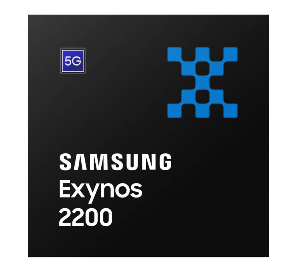
After multiple hiccups and rumors, Samsung has announced its next-gen Exynos 2200 SoC. Featuring the brand new Xclipse GPU based on AMD’s RDNA 2 graphics architecture, it’s the first mobile GPU to come with hardware-accelerated ray-tracing and variable rate shading (VRS). The SoC is fabbed on Samsung’s 4nm EUV process node and includes three different Arm core clusters: Cortex X2, A710, and A510 for performance-intensive, moderately demanding, and lightly threaded workloads, respectively.
The Exynos 2200 also packs an AI engine with a dual-core NPU and DSP and a 5G 7.35Gbps/5.1Gbps modem. The SoC supports up to a 4K/WQUXGA @ 120Hz or a QHD+ @ 144Hz display. 8K 60 FPS decoding is also fully supported with 10-bit H.265, and VP9/AV1 decode is also available. H265 decode at 8K 10-bit is supported at 30 FPS, similar to VP9. (Modafinil)
The processor features LPDDR5 memory which should keep the RDNA 2 GPU well-fed during intense gaming sessions. Samsung is positioning the Xclipse as a hybrid graphics processor between console and mobile gaming platforms. The “X” in Xclipse stands for Exynos while “eclipse” is meant to represent the end of the old era of mobile gaming.
Built on the most advanced 4-nanometer (nm) EUV (extreme ultraviolet lithography) process, and combined with cutting-edge mobile, GPU, and NPU technology, Samsung has crafted the Exynos 2200 to provide the finest experience for smartphone users. With the Xclipse, our new mobile GPU built with RDNA 2 graphics technology from the industry leader AMD, the Exynos 2200 will redefine the mobile gaming experience, aided by enhanced graphics and AI performance. As well as bringing the best mobile experience to the users, Samsung will continue its efforts to lead the journey in logic chip innovation.
Yongin Park, President of System LSI Business at Samsung Electronics
The AMD RDNA 2 graphics architecture at the heart of the Xclipse GPU is the primary attraction of Samsung’s next-gen Exynos SoC. Over the last few generations, the Korean chipmaker has been lagging behind Apple and Qualcomm in the PPA segment due to process or design issues. With the help of the cutting-edge Radeon IP, the plan is to one-up its American rivals.
With the high-performance AMD RDNA 2 architecture as its backbone, the Xclipse inherits advanced graphic features such as hardware-accelerated ray tracing (RT) and variable rate shading (VRS) that were previously only available on PCs, laptops, and consoles. It also comes with various technologies such as advanced multi-IP governor (AMIGO) that enhance overall performance and efficiency.
AMD RDNA 2 graphics architecture extends power-efficient, advanced graphics solutions to PCs, laptops, consoles, automobiles and now to mobile phones. Samsung’s Xclipse GPU is the first result of multiple planned generations of AMD RDNA graphics in Exynos SoCs. We can’t wait for mobile phone customers to experience the great gaming experiences based on our technology collaboration.
David Wang, Senior Vice President of Radeon Technologies Group at AMD
Earlier, Samsung had posted a tweet, teasing the launch of the Exynos 2200 on the 11th of Jan. Without any official word, the tweet was mysteriously deleted a couple of days prior to the reveal, fueling rumors (most likely true) of a thermal throttling issue.
We expect the Xclipse GPU to be clocked at 1.50GHz, lower than the initial target, but higher than what recent rumors claimed. Furthermore, don’t expect it to beat the Apple A15. It may end up outperforming the Snapdragon 8 Gen 1, but not by a large margin.
The Exynos 2200 is already in mass production and should be announced later this month or early next month along with a new Galaxy smartphone.
Previous coverage:
A while back, reputed tipster @Ice Universe (Twitter) revealed that the Exynos 2200 is the worst flagship SoC in its current state. Mediocre CPU performance and a thermally constricted GPU have left the 4nm SoC way behind its key rivals, namely Qualcomm and Apple. Both the A15 and the Snapdragon 8 Gen 1 offer considerably better GPU performance, with the Mali GPU on the MediaTek Dimensity 9000 managing to topple the Exynos as well.
The latest info from the source indicates that the original boost clock target for the RDNA 2 GPU on the Exynos 2200 was a respectable 1.9GHz. However, thermal throttling and overheating forced the engineers to scale it down to just 1.29GHz, marking a considerable regression in graphics performance. The team plans to optimize the RDNA 2 GPU for 1.49GHz but it’ll mostly be delegated to a lower-end device instead of the Galaxy S22.
Going through recent leaks on Twitter, tipsters have been surprisingly accurate with their figures on the Exynos 2200 and its RDNA 2 implementation. I’m genuinely curious as to whether the GPU failing to meet its pre-determined frequency targets on the Exynos 2200 is the result of Samsung’s node being inferior to TSMC’s 7nm/5nm for which the RDNA architecture was originally optimized.
Read more here:
