Samsung’s Exynos 2200 has gone from being one of the most anticipated SoCs of 2022 to an utter PR disaster. Featuring AMD’s RDNA 2 graphics IP, the processor was slated to bring accelerated gaming performance to the upcoming Galaxy S22 smartphone. Unfortunately, foundry problems paired with a communication lax has pretty much butchered the hype surrounding Samsung’s next-gen flagship processor.
A while back, reputed tipster @Ice Universe (Twitter) revealed that the Exynos 2200 is the worst flagship SoC in its current state. Mediocre CPU performance and a thermally constricted GPU have left the 4nm SoC way behind its key rivals, namely Qualcomm and Apple. Both the A15 and the Snapdragon 8 Gen 1 offer considerably better GPU performance, with the Mali GPU on the MediaTek Dimensity 9000 managing to topple the Exynos as well.


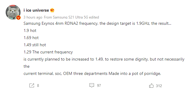
The latest info from the source indicates that the original boost clock target for the RDNA 2 GPU on the Exynos 2200 was a respectable 1.9GHz. However, thermal throttling and overheating forced the engineers to scale it down to just 1.29GHz, marking a considerable regression in graphics performance. The team plans to optimize the RDNA 2 GPU for 1.49GHz but it’ll mostly be delegated to a lower-end device instead of the Galaxy S22.
Going through recent leaks on Twitter, tipsters have been surprisingly accurate with their figures on the Exynos 2200 and its RDNA 2 implementation. I’m genuinely curious as to whether the GPU failing to meet its pre-determined frequency targets on the Exynos 2200 is the result of Samsung’s node being inferior to TSMC’s 7nm/5nm for which the RDNA architecture was originally optimized.
Previous coverage:
AMD’s mobile RDNA 2 GPU is capable of seriously high clock speeds. At the moment, the engineers are testing two variants of the Exynos 2200 SoC: one with the GPU core clock set to 1.29GHz, and the other to 1.58GHz. The catch is that with the latter, the CPU clocks (of the middle cores) have to be tuned down a bit to keep the TDP in check:
The source claims that the peak GPU score with the 1.58GHz variant is better due to higher retention even after throttling. It looks like the RDNA 2 architecture is capable of high boost clocks regardless of the process node. According to the latest rumor, the mobile RDNA 2 design Samsung is using is capable of a whopping 1.8GHz with the TDP set to 10W.
The scores of the mobile GPU in GFXBench are as follows:
The graphics processor integrated into the mobile SoC in partnership with AMD features 6 CUs, with an operating (boost?) clock of 1.31GHz. The processor was benchmarked (2nd round) in GFXBench, and the following scores were observed:
Manhattan 3.1: 170.7 FPS
Aztec Normal: 121.4 FPS
Aztec High: 51.5 FPS
The GFXBench figures from the 3rd round of the graphic throttling tests are as follows:
Manhattan 3.1: 127.5 FPS
Aztec Normal: 90.7 FPS
Aztec High: 39.65 FPS
Original post