A new patent published over at the Free Patent Online portal details a method to double the effective throughput of each SIMD (possibly) in AMD’s next-gen Radeon RX 7000 or the Instinct MI300 GPUs. Before we begin, it’s important to note that like all patents, this may or may not find its way into end hardware, so it’s in no way official. Let’s begin. We already know that AMD will be doubling the ALU count, and therefore, the number of SIMDs, and Compute Units (CU) per WGP in RDNA 3 for improved scalability. This particular patent appears to supplement that approach.
Now, whenever you increase the core count, you also need to ramp up the resources available to prevent them from starving, or in other ways avoid underutilization. This means more cache, more registers, larger buffers, and wider pipelines overall. According to this patent, AMD has found a way to double instruction throughput per SIMD32 (set of 32 ALUs or cores) by implementing two ALU pipelines per unit, per cycle and leveraging the cache to store the wavefronts (work items and thread data).

The wavefronts are supplied by the VGPRs (Vector General Purpose Registers) to the cache blocks every cycle without the need to expand their bandwidth or may even capacity. And once again, AMD delivers another breakthrough using, you said it, cache.
There are two scenarios that arise here. First, when the scheduler passes two instructions (from two separate waves) to the SIMD. In this case, one is executed at the first ALU pipeline and the other at the second, both at the same time. The wavefronts are copied from the cache and written back to the buffer, after which they are passed onto the registers.
Once again, you can see a similarity to the older GCN/CDNA architecture here where several waves are in motion simultaneously. Only, in this case, all the wavefronts are executed in one cycle rather than four (making an RDNA algorithm). It makes me wonder if AMD is fattening up the SIMDs or simply doubling their count per WGP.
In case you have a single instruction stream from only one wavefront, then the wavefront is split into two, the first half being sent to the first pipeline and the second half to the second pipeline. It’s worth noting that in the patent, this is a 64-work unit that is split into two 32 sub-waves, indicating that this could also be used with two SIMDs instead as well. Essentially, it would reduce the cost of increasing the core counts by cutting down on VGPRs and offloading that data to the cache.
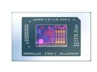
And then there’s this. The above image, AMD explains is an SoC featuring a CPU and GPU on the same package for a unified programming and execution environment. This has the MI300 written all over it which means in some form, this design may be utilized for both the next-generation of Radeon and Instinct GPUs. Here’s a flowchart explaining the entire process:
Source: FPO (via: Olrak)