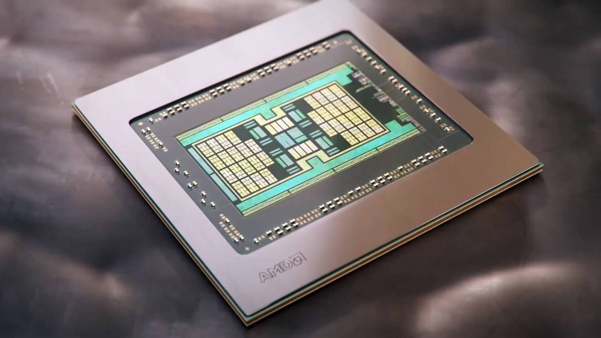
With the launch of the Big Navi graphics cards, AMD has finally returned to the high-end GPU space with a bang. While the RDNA 2 design is largely similar to RDNA 1 in terms of the compute and graphics pipelines, there are some changes that have allowed the inclusion of the Infinity Cache and the high boost clocks. In this post, we’ll talk about how the Navi GPUs are different from the traditional Vega and Polaris parts which were powered by the GCN architecture.
AMD’s GCN architecture powered Radeon graphics cards for almost a decade. Although the design had its strengths such as a powerful Compute Engine, hardware schedulers, and unified memory, it wasn’t very efficient for gaming. The hardware utilization was quite poor compared to contemporary NVIDIA parts, scaling dropped sharply after the first 11 CUs per shader engine, and overall, using more than 64 CUs per GPU wasn’t feasible.
As a result, despite featuring a powerful compute architecture, AMD’s GCN GPUs (Vega) repeatedly lost to NVIDIA’s high-end gaming products, all the while drawing significantly higher power.
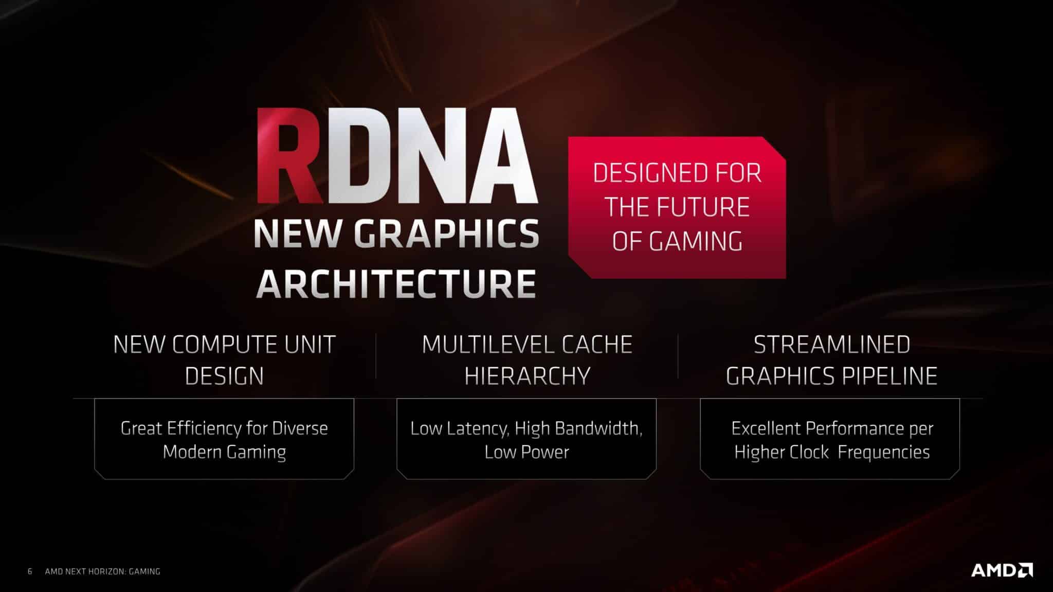
RDNA is the GPU architecture and Navi is the codename of the graphics processors built using it. Similarly, GCN was the architecture while Vega and Polaris are codenames.
The 1st Gen RDNA architecture powering the Navi 10 and Navi 14 GPUs (Radeon RX 5500 XT, 5600 XT, and 5700/XT) are based on the same building blocks as GCN: A vector processor with a few dedicated scalars for address calculation and control flow, separate compute and graphics pipelines running asynchronously. ALUs called stream processors provide the computational power, and the Command Processor (along with the ACEs) handles the workload scheduling per Compute Unit.
The core difference is that RDNA reorganizes the fundamental components of GCN for a higher IPC, lower latency, and better efficiency. That’s what Navi is all about: It does a lot more with notably less hardware!
AMD GCN: Powerful but Underutilized
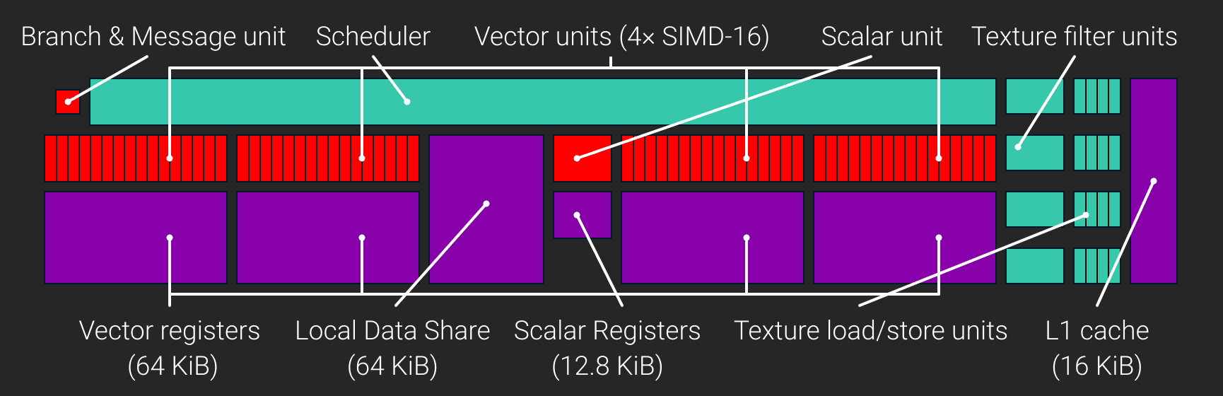
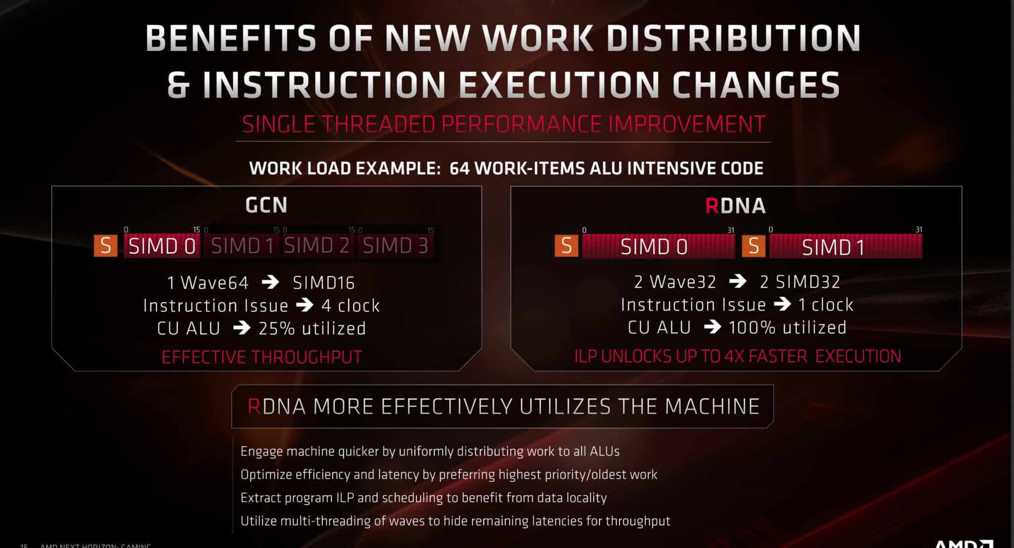
AMD’s GCN graphics architecture consisted of 64 wavefronts or work-items (and ALUs/cores) per Compute Unit. These were divided into four SIMDs (Single Instruction On Multiple Data Types), each packing 16 ALUs (SP).
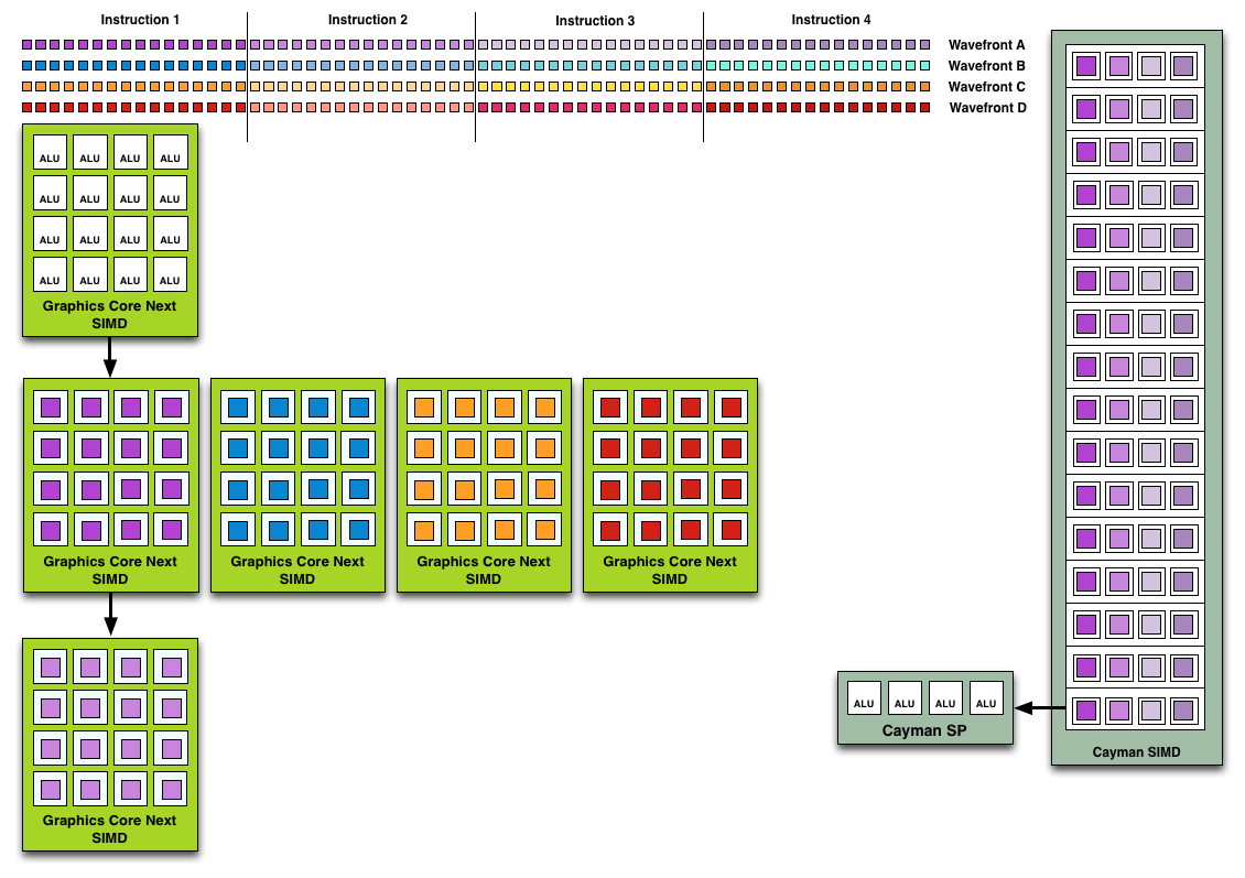
Here’s where most people get confused. Yes, it’s true that the scheduler could issue new wave groups after every four cycles, but at a time each Compute Unit would also work on four 64-item waves, not one 64-item wave. Like Bulldozer, the aim was to maximize parallelization. At the same time, GCN wasn’t an out-of-order architecture. The instructions within a wavefront were still executed as per their order. The difference was that the CU or SIMDs could switch to any of the four available waves.
The reason why this wasn’t very effective is that most games use shorter work queues due to which only one or two out of the four wavefronts were saturated per execution cycle. As a result, the competing NVIDIA GPUs with similar shader counts were much faster thanks to their Super-Scalar architecture and took only one to two cycles to execute these shorter dispatches. On the other hand, the AMD counterparts had to wait for four cycles for the next one despite having room for additional wavefronts.
Each vector can perform the same instruction on multiple data sets. The vector scheduling works on the basis that there will always be one instruction to be executed on multiple items. If there are only one or two sets available, the rest of the slots will be idle for that cycle.
SIMD
To sum up, like many other SIMD designs, a GCN Compute Unit worked on four wavefronts at a time and took four cycles to execute them. In an ideal world, this would mean that the effective time taken for one wave is one cycle. But, because of the way SIMDs works, this wasn’t the case and the CUs were often left underutilized.
AMD RDNA: Dual Compute Architecture and Wave32
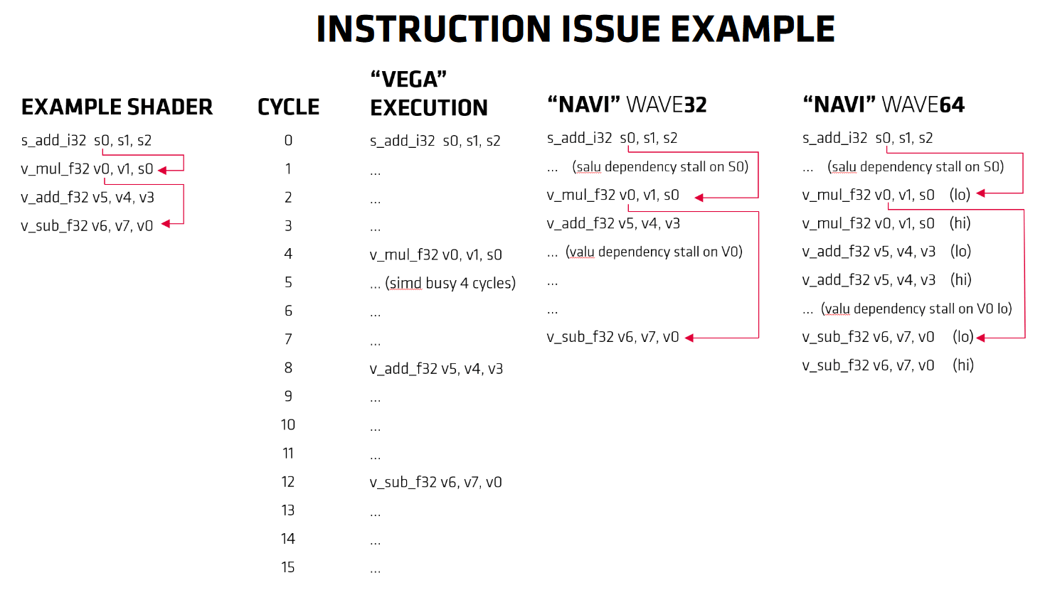
The RDNA architecture implemented in Navi uses wave32, a narrower wavefront with 32 work-items. It is much simpler and efficient than the older wave64 design. Each SIMD is wider but the Compute Units are narrower.
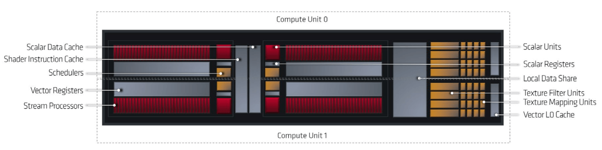
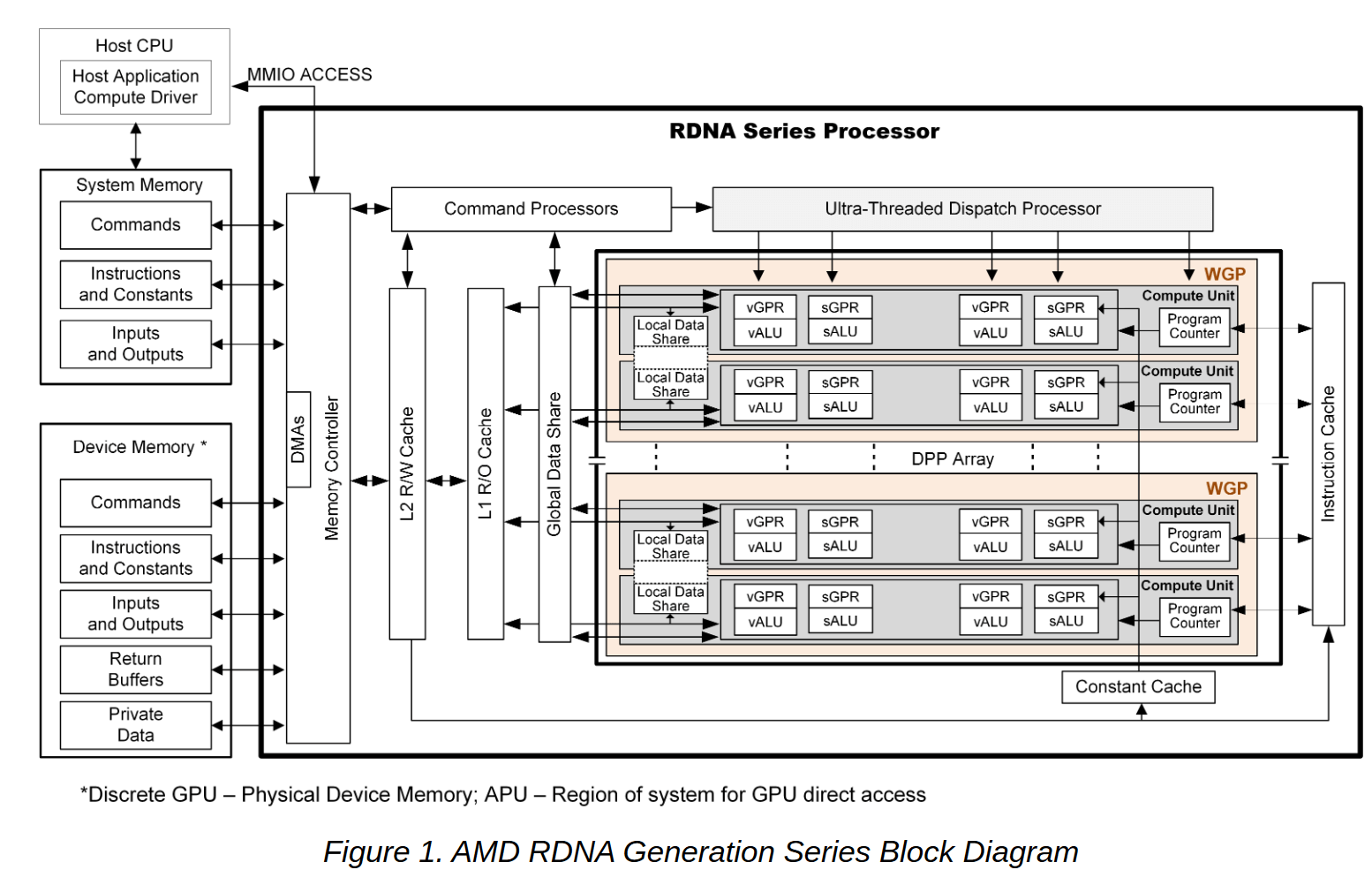
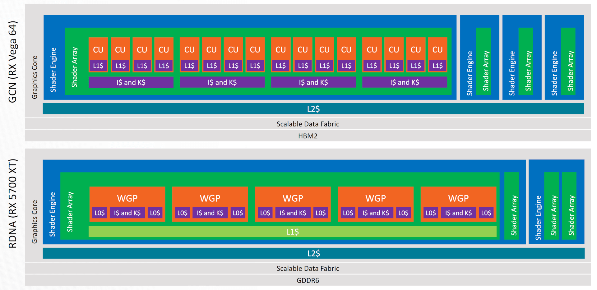
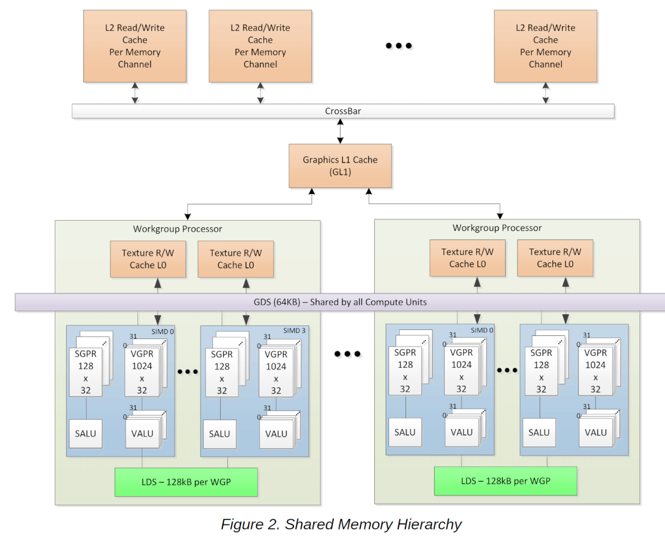
Where the Compute Unit was the basic shader unit in GCN, RDNA replaces it with a WGP (Work-Group processor): two CUs working in tandem with shared local data. The RDNA SIMDs consist of 32 shaders or ALUs, twice that of GCN. There are two SIMDs per CU and four in a Dual Compute Unit. The total number of stream processors in a CU is still 64, but they are distributed across two (not four) wider SIMDs. Refer to the Four cycles vs one cycle per instruction diagram further below.
The RDNA SIMDs consist of 32 shaders or ALUs, twice that of GCN. There are two SIMDs per CU and four in a Dual Compute Unit. The total number of stream processors in a CU is still 64, but they are distributed across two (not four) wider SIMDs.
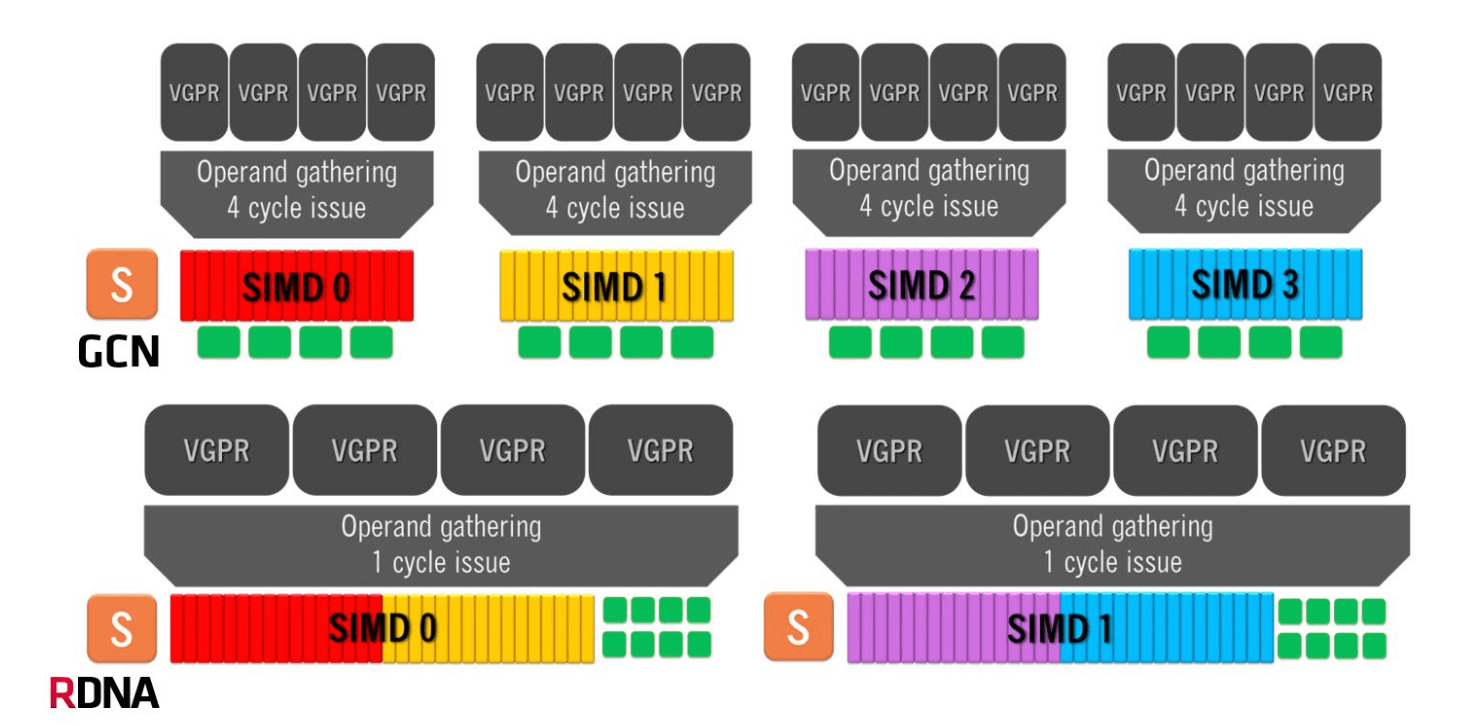
This arrangement allows the execution of one whole wavefront in one clock cycle, reducing bottlenecks and boosting IPC by 4x. By completing a wavefront 4x faster, the registers and cache are freed up much faster, allowing the scheduling of more instructions overall. Furthermore, wave32 uses half the number registers as wave64, reducing circuit complexity and costs too.
To accommodate the narrower wavefronts, the vector register file has also been reorganized. Each vector general-purpose register (vGPR) now contains 32 lanes that are 32-bits wide (for FP32), and an SIMD contains a total of 1,024 vGPRs – again, 4X the number of registers as in GCN.
Overall, the narrower wave32 mode increases the throughput by improving the IPC and the total number of concurrent wavefronts, resulting in significant performance and efficiency boosts.
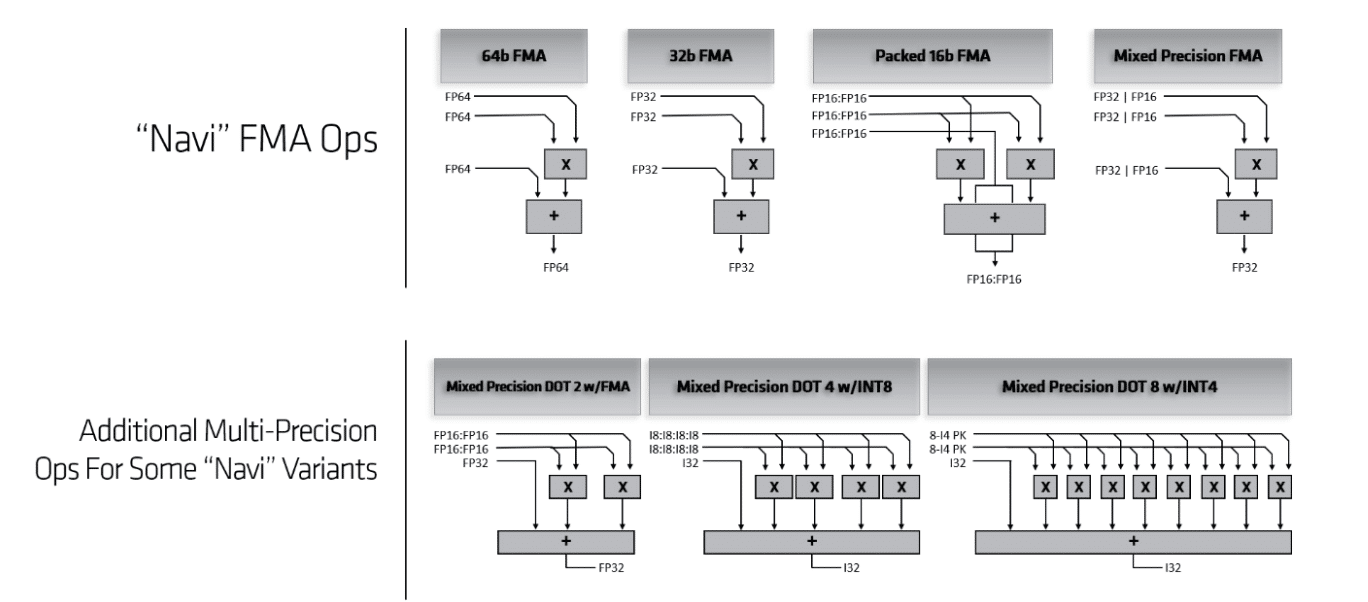
To ensure compatibility with the older GCN instruction set, the RDNA SIMDs in Navi support mixed-precision compute. This makes the new Navi GPUs suitable for not only gaming workloads (FP32), but also for scientific (FP64) and AI (FP16) applications. The RDNA SIMD improves latency by 2x in wave32 mode and by 44% in wave64 mode.
Asynchronous Compute Tunneling
One of the main highlights of the GCN architecture was the use of the Asynchronous Compute Engines way before NVIDIA integrated it into their graphics cards. RDNA retains that capability and doubles down on it.
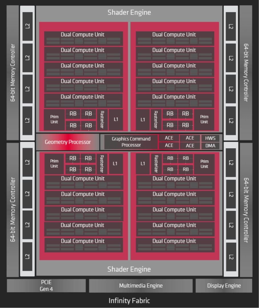
The Command Processor handles the commands from the API and then issues them to the respective pipelines: The Graphics Command Processor manages the graphics pipeline (shaders and fixed-function hardware) while the four Asynchronous Compute Engines (ACE) take care of the Compute. The Navi 10 die (RX 5700 XT) has one Graphics Command Processor and four ACEs. Each ACE has a distinct command stream while the GCP has individual streams for every shader type (domain, vertex, pixel, raster, etc).
In GCN, the command processor could prioritize compute over graphics. In the RDNA architecture, the GPU can completely suspend the graphics pipelines, using all the resources for high-priority compute tasks.
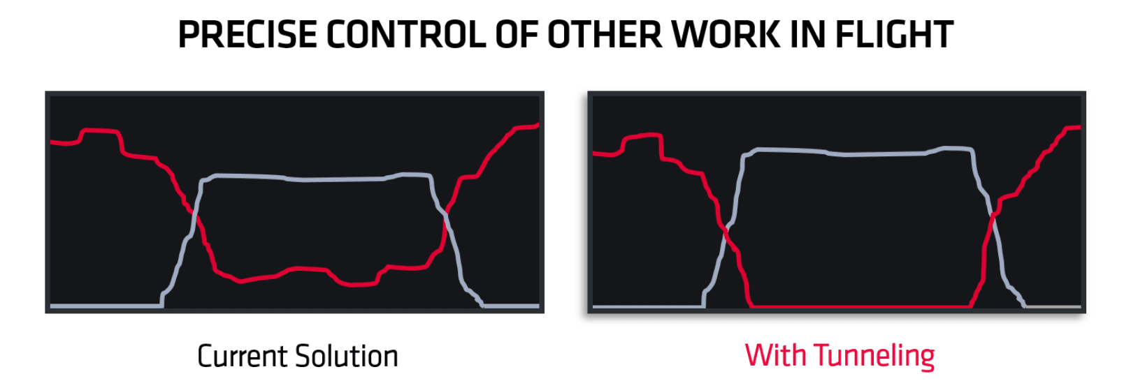
The RDNA architecture improves parallel processing at an instruction level by introducing a new feature called Asynchronous Compute Tunneling. Both GCN and the newer Navi GPUs support asynchronous compute (simultaneous execution of graphics and compute pipelines), but RDNA takes a step further. At times when one task (graphics or compute) becomes far more latency-sensitive than the other, Navi has the ability to completely suspend the latter.
In GCN based Vega designs, the command processor could prioritize compute over graphics and spend less time on shaders. In the RDNA architecture, the GPU can completely suspend the graphics pipelines, using all the resources for high-priority compute tasks. This significantly improves performance in the most latency-sensitive workloads such as virtual reality.
Scalar Execution for Control Flow
Continued on the next page…
Most of the computation in AMD’s GCN and RDNA architectures is performed by the SIMDs which happen to be vector in nature: perform a single instruction on multiple data types (32 INT/32 FP executed per SIMD per cycle, simultaneously). However, there are scalar units in each CU as well. Each Compute Unit in RDNA 1 can launch (dispatch) four instructions per cycle, two scalars, two vectors. Within an RDNA1 WGP, the total throughput is 128 vectors and 4 scalars per clock. Each of the four SIMDs contributes equally to that figure.
Each SIMD contains a 10KB scalar register file, with 128 entries for each of the 20 wavefronts. A register is 32-bits wide and can hold packed 16-bit data (integer or floating-point) and adjacent register pairs hold 64-bit data. The scalars are used for address generation for the load/store units and manage the SIMD control flow.
When a wavefront is initiated, the scalar register file can preload up to 32 user registers to pass constants, avoiding explicit load instructions and reducing the launch time for wavefronts.
The 16KB write-back scalar cache is 4-way associative and built from two banks of 128 cache lines that are 64B each. Each bank can read a full cache line, and the cache can deliver 16B per clock to the scalar register file in each SIMD. For graphics shaders, the scalar cache is commonly used to stored constants and work-item independent variables.
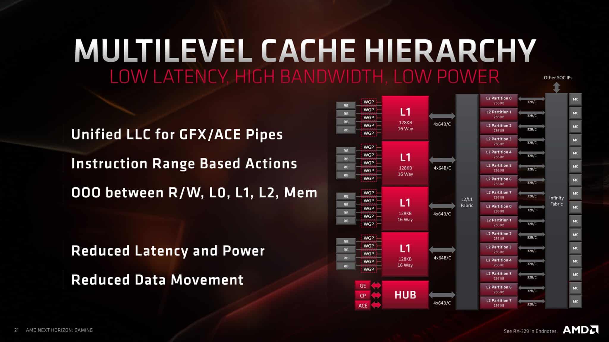
Cache: L0 & Shared L1
While the old GCN and rival NVIDIA GPUs rely on two levels of cache: RDNA adds a third L1 cache in the Navi GPUs. Where the L0 cache is private to a DCU, the L1 cache is shared across a group of Dual Compute Units. This reduces costs, latency, and power consumption. It reduces the load on the L2 cache. In GCN, all the cache misses of the per-core L1 cache were handled by the L2 cache. In RDNA, the new L1 cache centralizes all caching functions within each shader array.
While the L0 cache is private to a DCU, the L1 cache is shared across a group of Dual Compute Units.
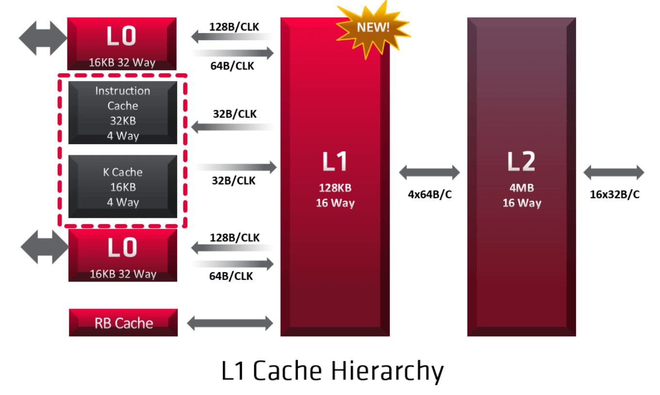
Any cache misses that happen in the L0 caches pass to the L1 cache. This includes all the data from the instruction, scalar, and vector caches, in addition to the pixel cache. L1 is a read-only cache and each is composed of four banks, resulting in a total of 128KB. It is a 16-way set-associative cache memory. The L1 cache is backed by the L2; a write to L1 will be invalidated and copied to L2 or memory.
The L1 cache controller coordinates memory requests and forwards four per clock cycle, one to each L1 bank. Like in any other cache memory, L1 misses are serviced by the L2 cache.
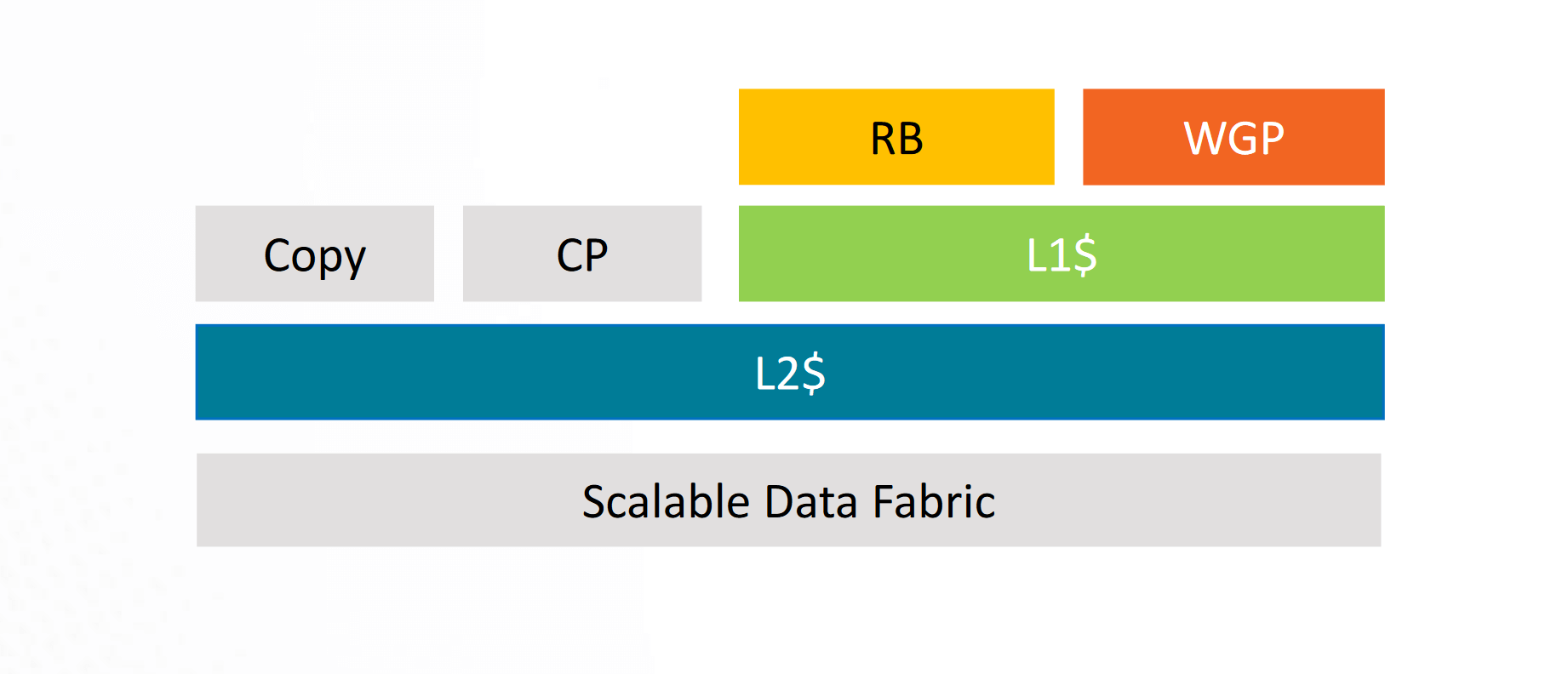
On the Polaris GPUs, only the Compute Units were the clients of the L2 cache. The RBs, Copy Engine, and CP wrote directly to the memory, resulting in lots of L2 flushes. Vega refined this design by making the RBs clients of the L2 as well, thereby reducing L2 flushes. RDNA and Navi go a step ahead of the GCN derivatives by making the copy engine a client of L2 as well. This should result in very few L2 flushes.
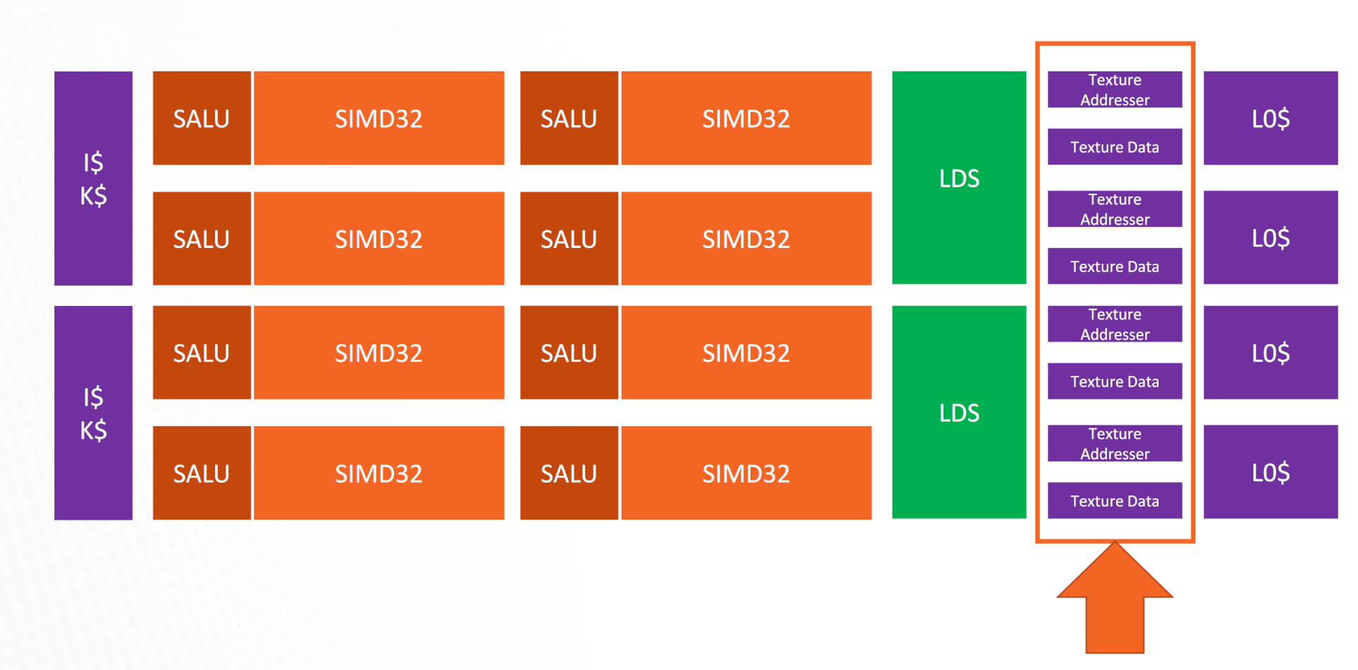
Dual Compute Unit Front End
Each Compute Unit fetches instructions via the Instruction Memory Fetch. In GCN, the instruction cache was shared between four CUs, but in RDNA (Navi), the L0 instruction cache is shared amongst the four SIMDs in a Dual CU. The instruction cache is 32KB and 4-way set-associative. Like the L1, it is organized into four banks of 128 cache lines, each 64-bytes long.
In GCN, the instruction cache was shared between four CUs, but in RDNA (Navi), the L0 instruction cache is shared amongst the four SIMDs in a Dual CU.
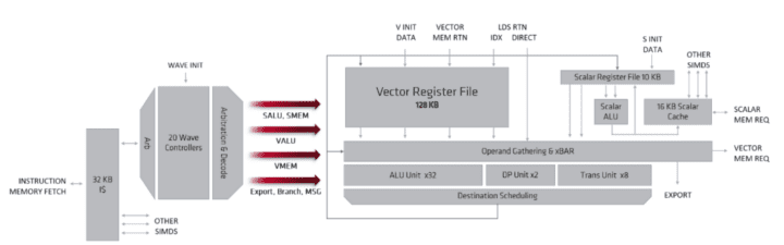
The fetched instructions are deposited into the wavefront controllers. Each SIMD has a separate instruction pointer and a 20-entry wavefront controller, for a total of 80 wavefronts per dual compute unit. Wavefronts may be different from a work group or kernel. Although a higher number of wavefronts may be fetched, a dual-compute unit works on only two wave32 workgroups simultaneously.
As already mentioned, where GCN requested instructions once every four cycles, Navi does it every cycle (2-4 ins per cycle). After that, each SIMD in an RDNA based Navi GPU can decode and issue instructions every cycle as well, increasing the throughput and reducing latency by 4x over GCN.
To accommodate the new wave32 mode, the cache and memory pipelines in each RDNA SIMD have also been revamped. The pipeline width has been doubled compared to GCN-based Vega GPUs. Every SIMD has a 32-wide request bus that can transmit the address for a work-item in a wavefront directly to the ALUs or the vGPRs (Vector General Purpose Registers).
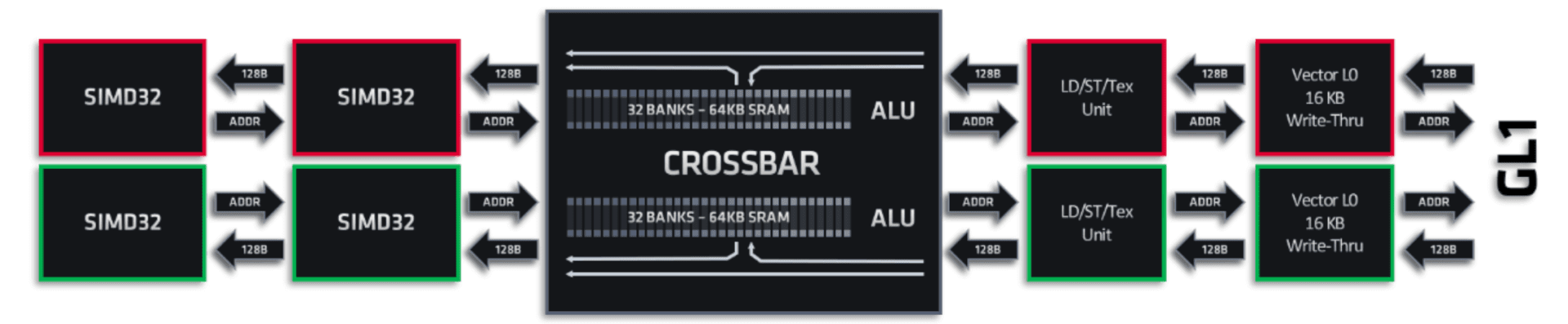
A pair of SIMDs share a request and return bus, however, a single SIMD can receive two chunks of 128B cache lines per clock: one from the LDS (Load-Store) and the other from the Vector L0 cache.
Render Back End (RBs) and Texture Units
The final fixed-function graphics stage in an RDNA based Navi GPU is the Render Backend (RB), which performs depth, stencil, and alpha tests and blends pixels for anti-aliasing and other final tests. Each of the RBs in the shader array can test, sample, and blend pixels at a rate of four output pixels per clock. The major improvement in the RDNA architecture here is that the RBs access data through the graphics L1 cache, which reduces the pressure on the L2 cache and saves power by moving fewer data. Recall, how in GCN, the RBs wrote data directly to the memory, then in Vega via the L2 cache.
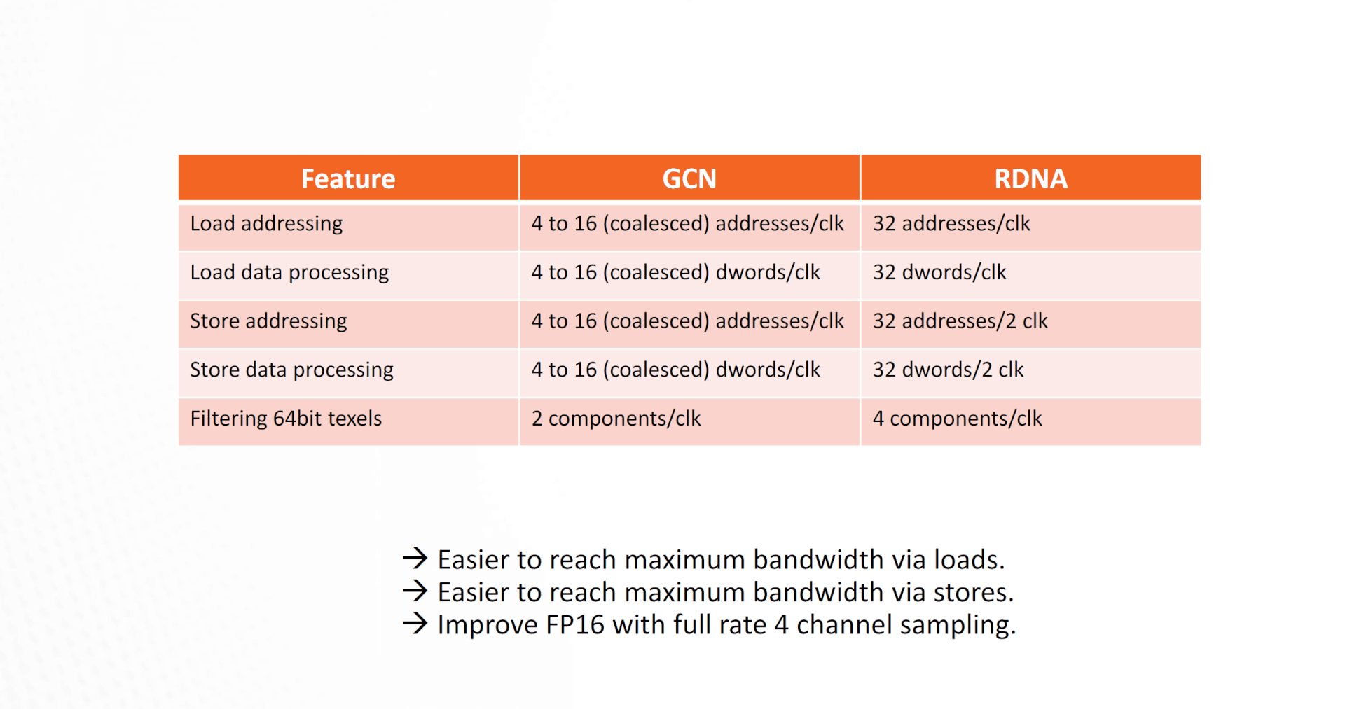
The Texture Units have also received a significant uplift with RDNA and Navi. The load and store processing speeds are multiple times faster compared to GCN, making it easier for the GPU to reach maximum bandwidth via both loads and stores.
RDNA vs GCN: ALU Utilization Comparison
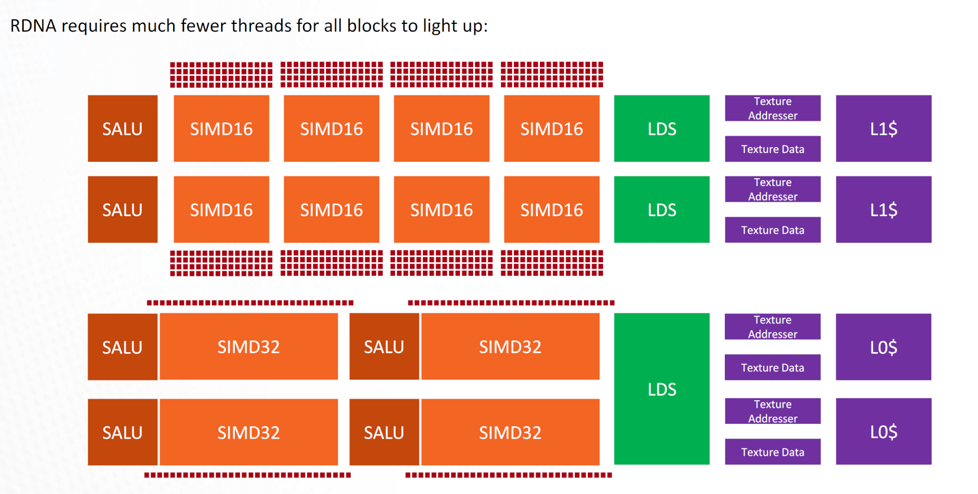
It’s much easier to saturate the SIMDs and thereby the WGPs on Navi (RDNA) compared to GCN. One WGP (2 CUs) requires just (4 SIMDs *32 items) 128 threads to reach 100% ALU utilization. GCN, on the other hand, needed (2 CUs * 4 SIMDs * 65 items) 512 threads to reach 100% utilization. That’s four times as much!
Video Encode and Decode
Like NVIDIA’s Turing encoder, the Navi GPUs also feature a specialized engine for video encoding and decoding.
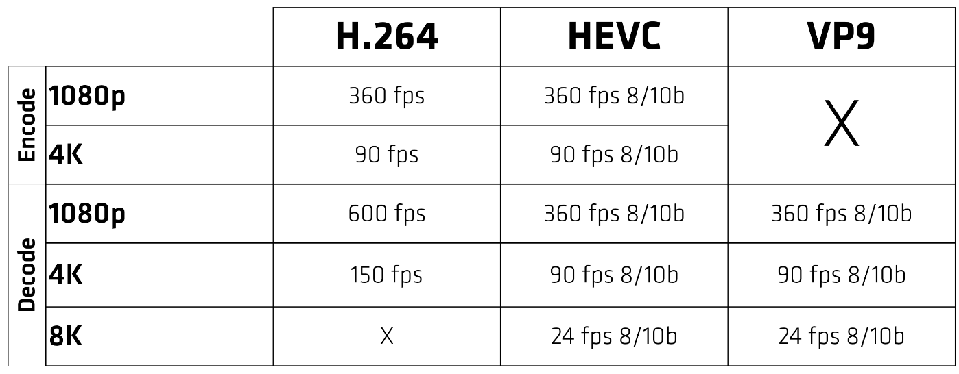
In Navi 10 (RX 5600 & 5700), unlike Vega, the video engine supports VP9 decoding. H.264 streams can be decoded at 600 frames/sec for 1080p and 4K at 150 fps. It can simultaneously encode at about half the speed: 1080p at 360 fps and 4K at 90 fps. 8K decode is available at 24 fps for both HVEC and VP9.
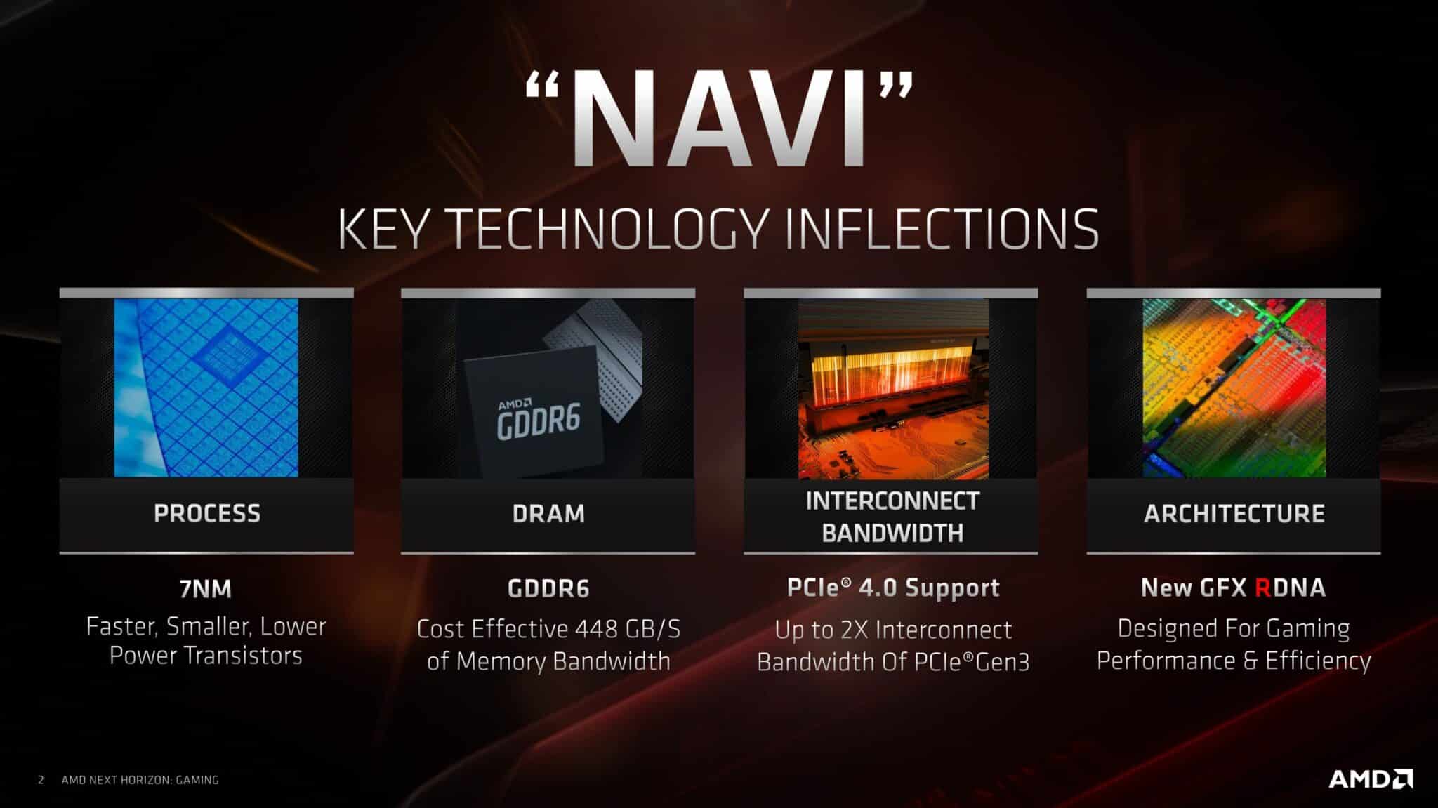
7nm Process and GDDR6 Memory Standard
While the 7nm node and GDDR6 memory are often advertised as part of the new architecture, these are third-party technologies and aren’t exactly part of the RDNA micro-architecture. The GPUs are, however, optimized to take maximum advantage of these technologies.
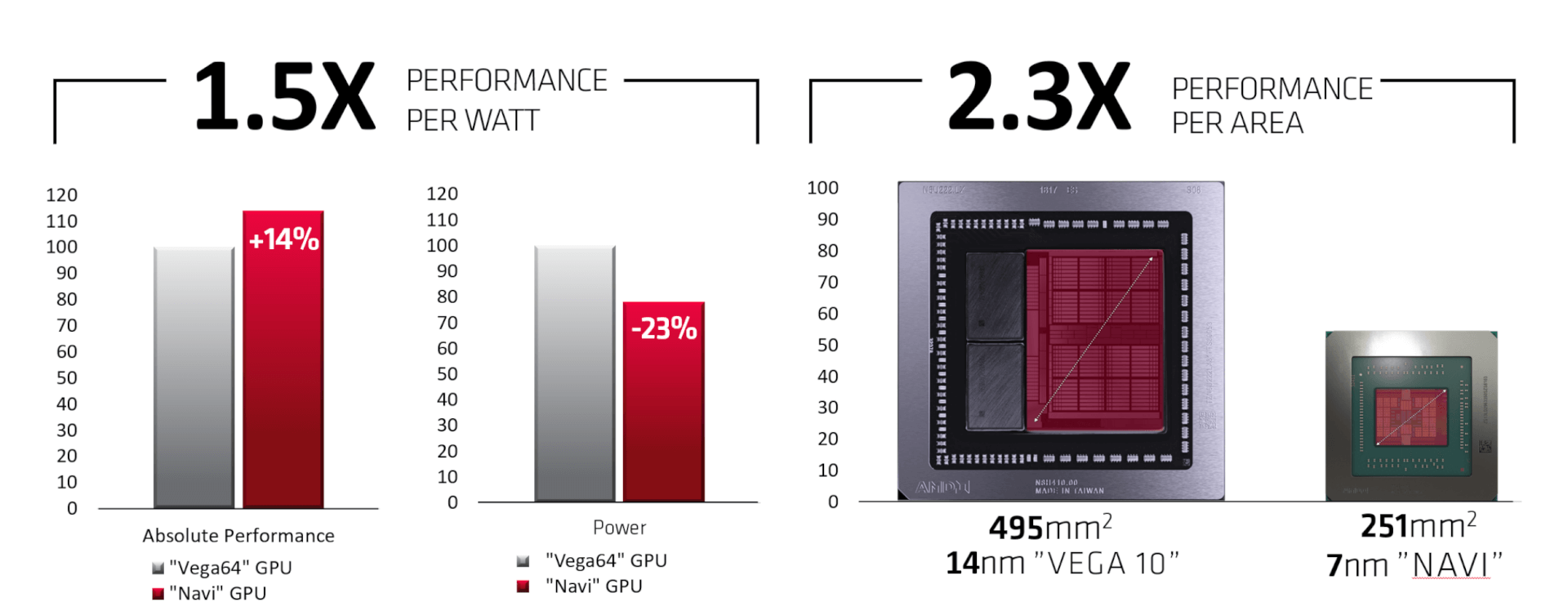
TSMC’s 7nm node does, however, improve the performance per watt significantly over the older 14nm process powering the older GCN designs, namely Polaris and Vega. It increases the performance per area by 2.3x and the performance per watt metric is boosted by 1.5x.
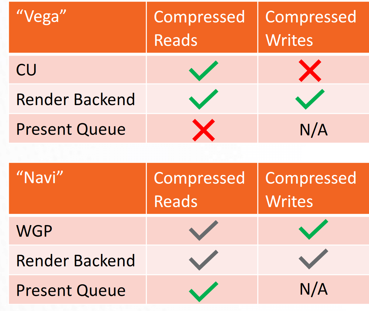
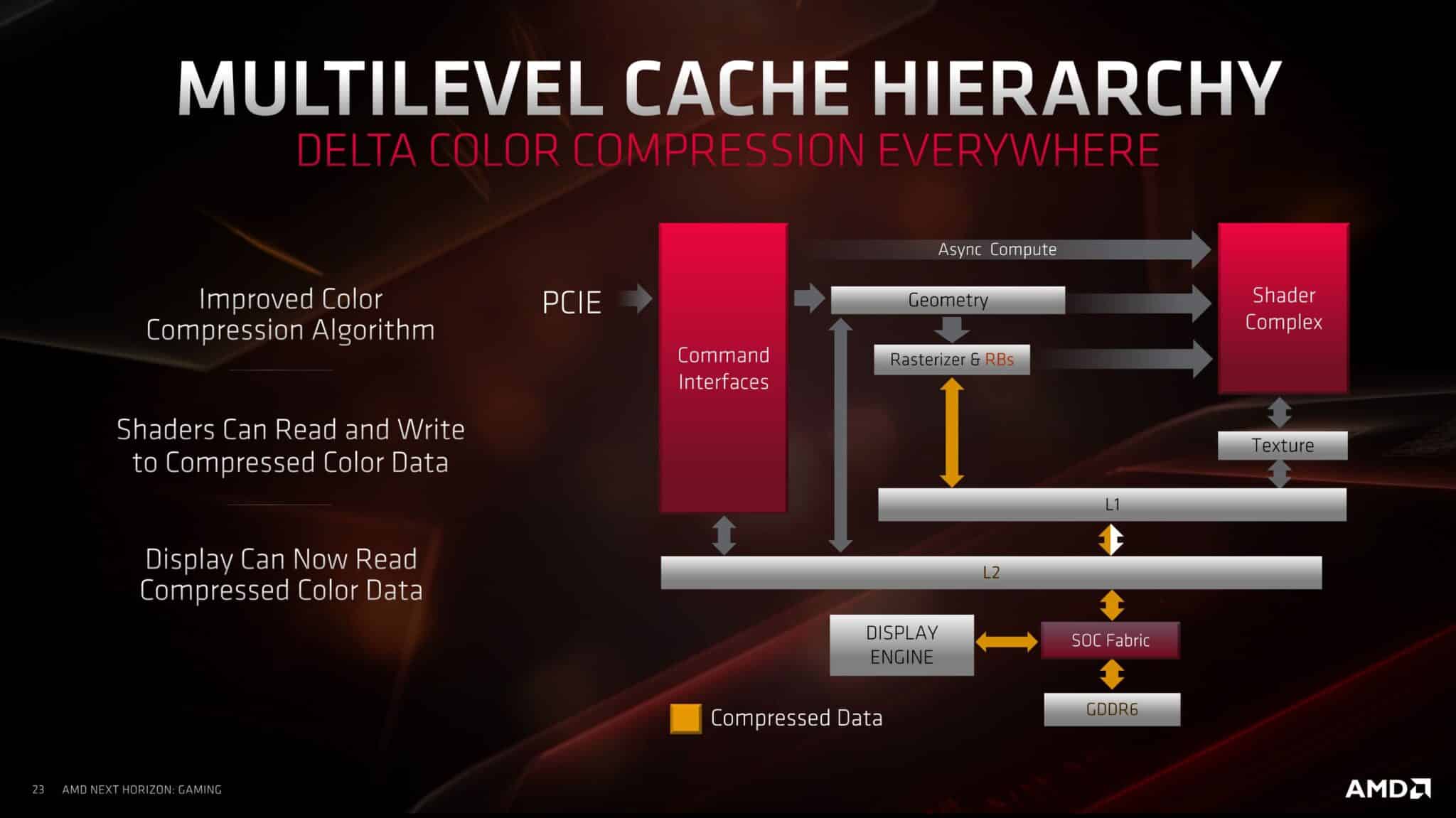
To maximize the bandwidth, data compression has been aggressively added wherever possible. While GCN and Navi did only compressed reads and writes in the RBs, Navi expands the latter to the CUs, in addition, to implementing it in the present queue as well.
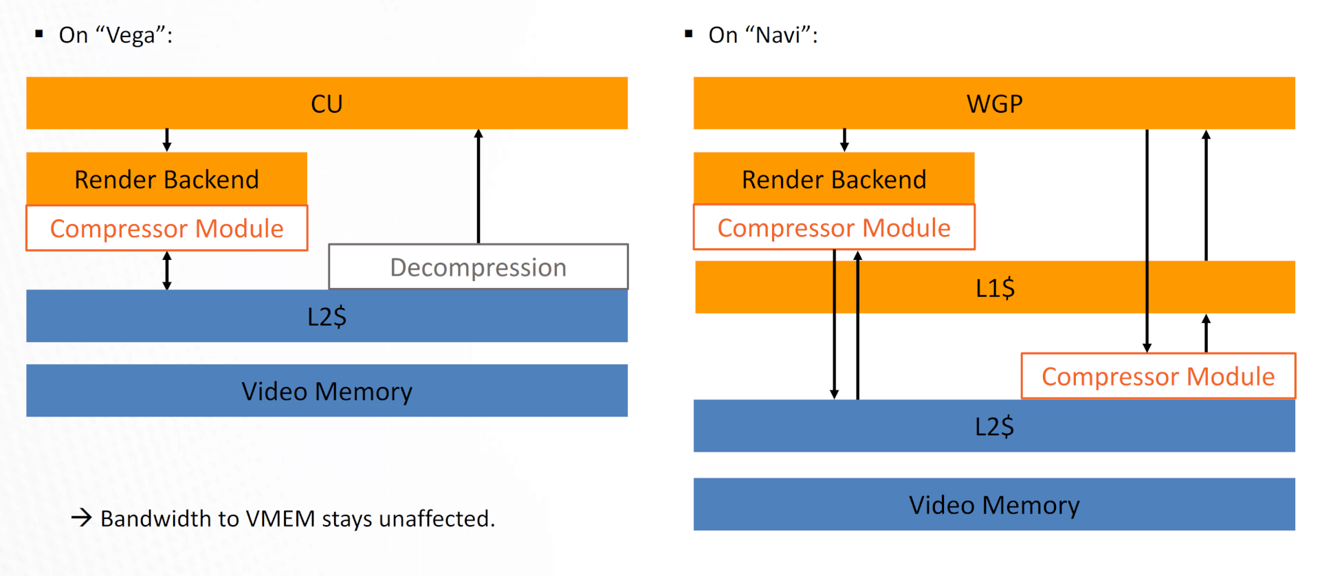
Now, there’s a compressor module between the WGP (CUs) and the L2 cache, in addition to the RBs. Vega was lacking the former, and data compression was limited to reads from the L2.
Conclusion
As you can see, while RDNA and Navi don’t exactly reinvent the Radeon design, they mainly just refine it. The pipeline bottlenecks have been removed, latency has been decreased and every SIMD is now wider and faster. There are more Render Backends per Shader Engine, with three levels of unified cache, a major step up from the preceding Vega GPUs. It’ll be interesting to see how different RDNA 2 will be from the existing Navi GPUs. To be honest, I don’t think there will be any radical changes. There might be some dedicated cores for ray-tracing acceleration or upscaling and that’s about it. What AMD needs to work on is their software and drivers.
-
 AMD Radeon RX 7900 XT Drops Below $700 (-$210 Off), RX 6800 at $369 (-$310 Off)
-
 AMD Radeon RX 9900 XTX to Feature 18432 Cores/288 CUs: Replaces the Shelved 8900 XTX
-
 AMD Radeon RX 8900 XTX Specs: 13000+ Cores for the Cancelled RDNA 4 Flagship
-
 NVIDIA RTX 4080 vs 4080 Super vs 4090: 34 Benchmark Comparisons