Intel has been following a monolithic approach to processor design. Essentially, this means that all cores, cache, and I/O resources for a given processor are physically on the same monolithic chip. There are some clear advantages to this approach.
The most notable is reduced latency. Since everything is on the same physical substrate, different cores take much less time to communicate, access the cache, and access system memory. Latency is reduced. This leads to optimal performance.


If everything else is the same, the monolithic approach will always net you the best performance. There’s a big drawback, though. This is in terms of cost and scaling. We need to take a quick look now at the economics of silicon yields. Strap in: things are going to get a little complicated.
Defects and Yields
When foundries manufacture CPUs (or any piece of silicon), they rarely manage 100 percent yields. Yields refer to the proportion of usable parts made. If you’re on a mature process node like TSMC’s N7 (7nm), your silicon yields will be more than 80%. You get a lot of usable CPUs with minimal wastage. The inverse is that for every 10 CPUs you manufacture, you have to discard at least 2-3 defective units. The discarded unit costs money to make, so that cost has to factor into the final selling price.
At low core counts, a monolithic approach works fine. This largely explains why Intel’s mainstream consumer CPU line has, until Ryzen, topped out at 4 cores. Increasing the core count on a monolithic chip dramatically increases costs.
On a high-end monolithic die, every (or nearly every) core has to be functional. If you’re fabbing an eight-core chip and 7 out of 8 cores work, you still can’t use it. Remember what we said about yields being more than 80 percent?
Mathematically, that ten percent defect rate stacks for every additional core on a monolithic die to the point that with, say, a 28-core Xeon, Intel has to throw away one or two defective chips for every usable one since all 28 cores have to be functional. Costs don’t just scale linearly with core count–they scale exponentially because of wastage.
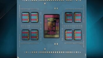
The economics are much more forgivable with the chiplet approach, as costs scale linearly with core counts. Because AMD’s wastage rate is relative to its ability to create a functional 4-core block at most (a single CCX), they don’t have to throw out massive stocks of defective CPUs.
The second advantage comes from their ability to leverage those defective CPUs themselves. Whereas Intel mostly throws them out, AMD disables functional cores on a per-CCX basis to achieve different core counts.
Chiplet or Monolithic: Which is Better?
The chiplet approach is going to see widespread adoption in the coming years, from both AMD as well as Intel, for CPUs as well as GPUs. Moore’s law–which mandated a doubling in processing power, mainly due to die shrinks (56nm to 28nm> 28nm to 14nm>14nm to 7nm) every couple of years–has comprehensively slowed down.
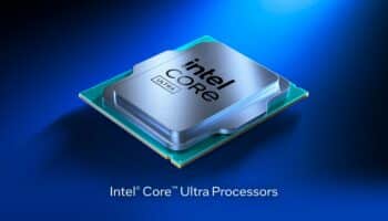
Intel released its first major chipped or tiled CPUs as Xeon Sapphire Rapids a while back. The 14th Gen Core processors codenamed “Meteor Lake” will be the first chiplet lineup from Team Blue. They are expected to hit the market in the final quarter of 2023.