The latest info from @Greymon (Twitter) suggests that AMD’s next-gen RDNA 3 based Navi 33 GPU will have fewer cores than initially anticipated. In previous rumors, the same source had stated that the Navi 33 die would pack up to 5,120 cores or 20 WGPs, but in a recent update, he suggests that the GPU will top out at 4096 shaders (stream processors).
That’s a notable drop from the originally anticipated figure and perhaps an expected change. It’s worth noting that Navi 33 will power the Radeon RX 7600 XT part, making it a massive upgrade over the existing Radeon RX 6600 XT and its 2,304 shaders. We’re looking at an increase of more than 2x if you include the IPC, compute, and frequency gains.


Originally, the Navi 33 die was expected to feature 2 shader engines, each with 2 shader arrays (4 overall). Each shader array consisted of 5 WGPs (20 overall), and each WGP has 8 SIMD32 units with 32 ALUs (80 per SE/160 overall). This resulted in a shader count of 5120 cores, the same as the RX 6900 XT (Navi 21).
The new numbers are more realistic and paint the RDNA 3 based Navi 33 GPU having a total of 16 WGPs or 4096 stream processors. Regardless, we’re looking at a raw compute gain of 75%. Pair that with the IPC and node-related frequency increases, and we can easily expect an overall performance gain of 2x over the 6600 XT.
The Radeon RX 7600 XT (Navi 33) is expected to pack 256 MB of Infinity Cache. Rumors indicate two GCDs, each with two 32-bit memory controllers. That results in a total of four 32-bit memory controllers for an overall bus width of 128-bit.
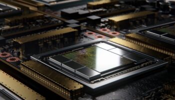
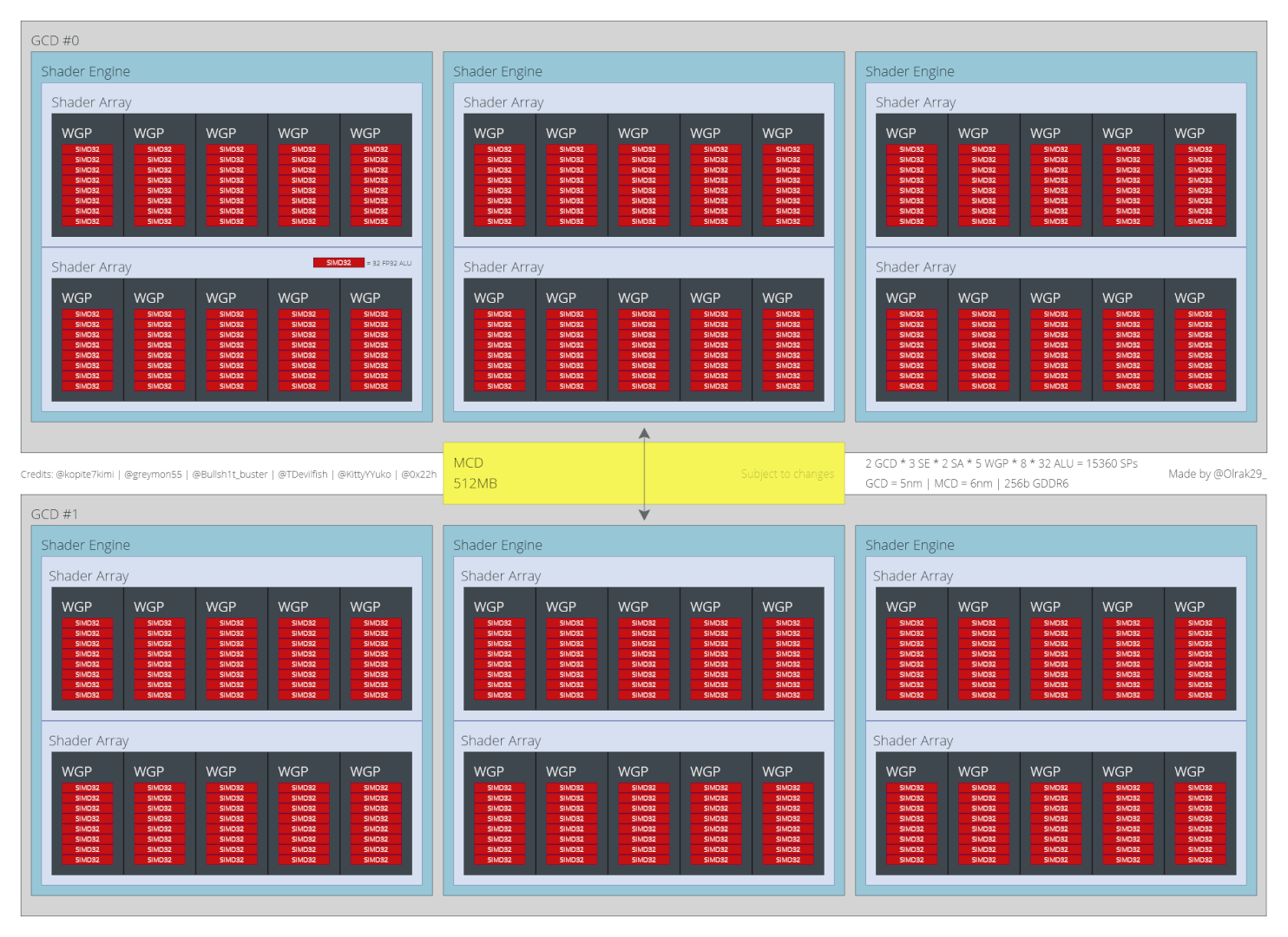
With Navi 31, each Graphics Die (GCD) features three Shader Engines which are made up of two Shader Arrays each. In turn, each Shader Array packs five WGPs containing eight SIMD units (vs four on RDNA 2). The two dies are connected by a bridge interconnect paired with 512MB of L3 “Infinity” Cache. According to the source, the GCDs will be fabbed on TSMC’s 5nm (N5) node while the MCD will be fabbed on the older 6nm (N6) node. Each die should come with a 128-bit bus (divided into eight controllers), resulting in an overall bus width of 256-bit and the same external bandwidth of 448GB/s as the RX 6800 XT/6900XT.
In comparison, Navi 21 featured a Shader Engine packing 10 Dual Compute Units (20 Compute Units) which was in turn divided into two SIMDs per CU or four per DCU. Each CU featured its own vector and scalar units, along with a ray-accelerator, texture mapping units, registers, and cache. Scheduling was done on a WGP (DCU) basis, meaning four wave32 workgroups were assigned at a time. With Navi 3x, scheduling will become more complex as you’re taking 8 SIMDs or wave32 workgroups into account at once.