AMD allegedly canceled its RDNA 4 flagship, the Radeon RX 8900 XTX, early last year. According to rumors (Moore’s Law is Dead), the Navi 4C GPU featured a modular design with up to 14 chiplets (dies/tiles) packaged using TSMC’s CoWoS technology. The RX 8900 XTX consisted of three Active Interposer Dies AIDs and one Multimedia and I/O Die (MID) connected using a CoWoS-L silicon bridge. The interposer dies are linked to the substrate using C4 bumps.
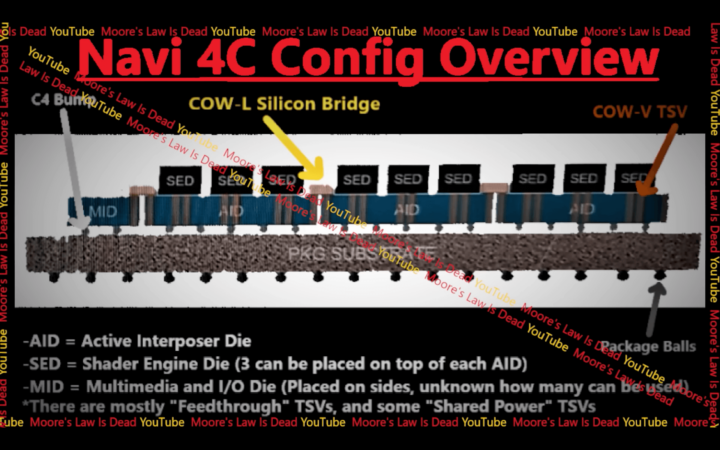
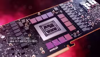
The Multimedia and I/O Die (MID) played the same role as the MCD (Memory Complex Dies) found on the Radeon RX 7900/7800 series GPUs. It houses the memory controllers, the corresponding L3 “Infinity Cache” and other I/O devices.


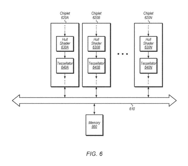
The Shader Engine Dies (SEDs) are placed at the top of the Active Interposers using 3D packaging. Each AID holds three SEDs, connected using CoWS-V TSVs. A fully enabled Navi 4C GPU was going to feature up to 9 Shader Dies, with a few disabled for the RX 8900 XTX. This was a remarkable modular design, likely with plenty of shared points with the Instinct MI300.
However, unlike training/inferencing workloads, gaming is extremely sensitive to latency. AMD overcame the latency issue with the MCDs on Navi 31 and 32 by increasing Infinity Fabric clocks. Doing the same with multiple compute dies is highly complicated as they feature more than just DRAM and high-level cache. Synchronizing 9 disaggregated shader units with several choke points was the challenge that undid the RX 8900 XTX (Navi 4C).
AMD Patent Explaining a Complex Chiplet GPU Architecture
In December, we spotted an AMD patent describing the functioning of a highly complex chiplet architecture. The patent explains a highly flexible chiplet GPU architecture consisting of up to 12 dies working in parallel without a central or master die. It breaks down the work distribution between chiplets consisting of specialized blocks, including the command processor, geometry engine, shader engine, and rasterizers.
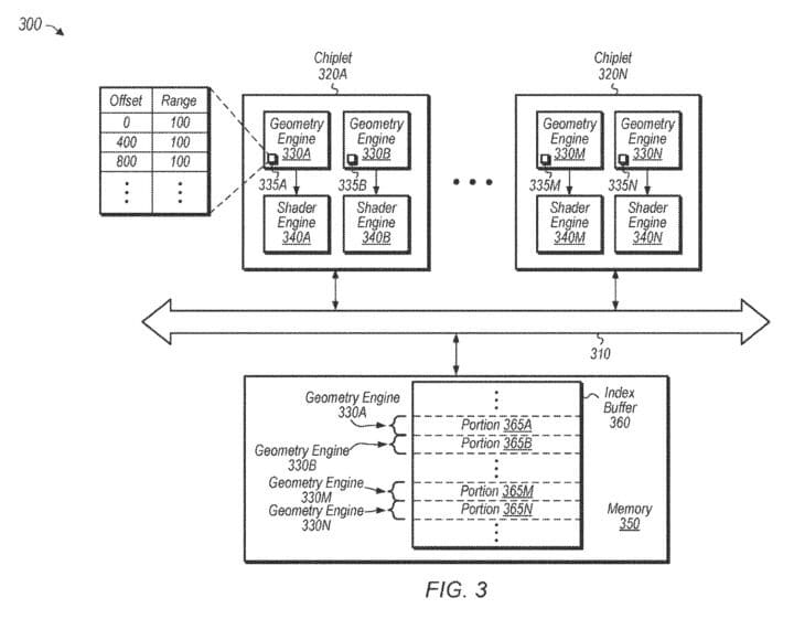
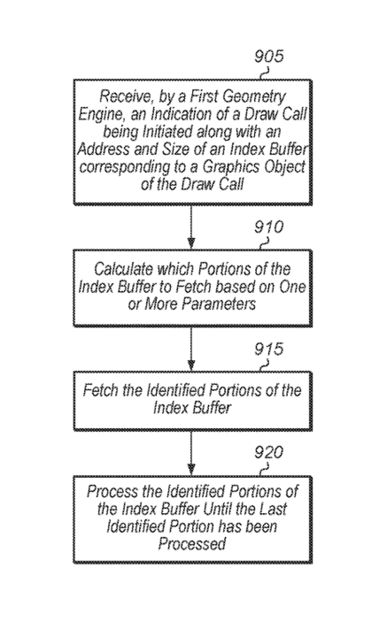
Each die executes its respective indices independently. When a draw call is issued, the first geometry engine calculates the portions of the index buffer to be fetched. This can be based on the number of geometry engines working on the draw call, the IDs, the number of indices to fetch for each portion, etc. This allows the calculation of the portions of the index buffer locally and independently on the various geometry engines and in parallel.
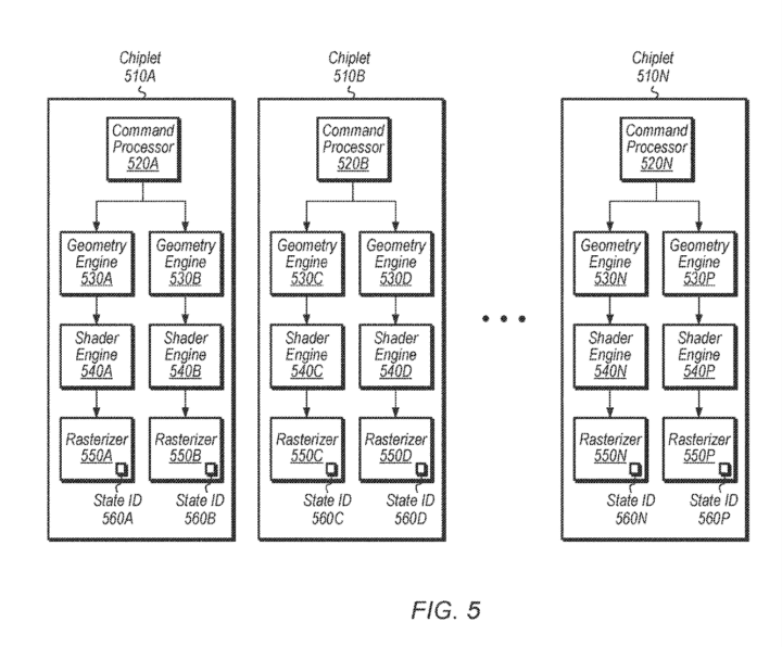
The CPU communicates with the main memory and the GPU chiplets via the PCIe bus. The chiplets themselves are connected using the Infinity Fabric. The applications running on the CPUs see the chiplets as a single entity, with the firmware being the only component capable of distinguishing between them.
The patent explains ways to distribute work between geometry engines. In one of them, the number of indices per portion is determined using the size of the primitive group. The size depends on the primitive type. Each geometry engine calculates its indices to process independently of the rest, allowing parallel execution without synchronization or barriers.
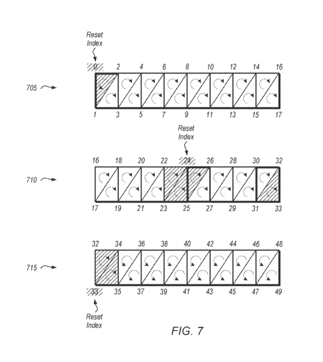
The below figure illustrates the drawing of three different strips by separate geometry engines. The shaded primitives are dropped due to the index reset, and the dotted arc indicates the direction of the winding order. Index resets reverse the direction of the winding order from counter-clockwise to clockwise or vice versa.
Another method involves the synchronization of the disaggregated chiplets. For every draw call, each command processor generates a state ID corresponding to the numerous pipelines (processing stages) carried out by the chiplets.
Much of the chiplet GPU patent breaks down ways to distribute the indices between the geometry engines (chiplets). In one instance, the command processor is paired with two pipelines. Consequently, its geometry, shader engines, and rasterizers are linked to one pipeline each. Similarly, the remaining chiplets work on two pipelines in parallel.
The rest of the patent discusses the partitioning of draw calls and primitives between the numerous chiplets. The arrangement has to be such that the latency penalty and queue divergence are minimal. The shader engines on different dies need to be adequately utilized and synchronized without the need to share data across the interconnect.
Temporal accumulation was the death of SLI and XFX, and there’s little chance for a chiplet GPU unless these issues are addressed. From the look of things, I’d say that we’re still at least two generations away from a chiplet GPU. The Radeon RX 8900 XTX has allegedly been canceled, leaving RDNA 4 with budget and midrange monolithic designs.