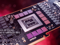
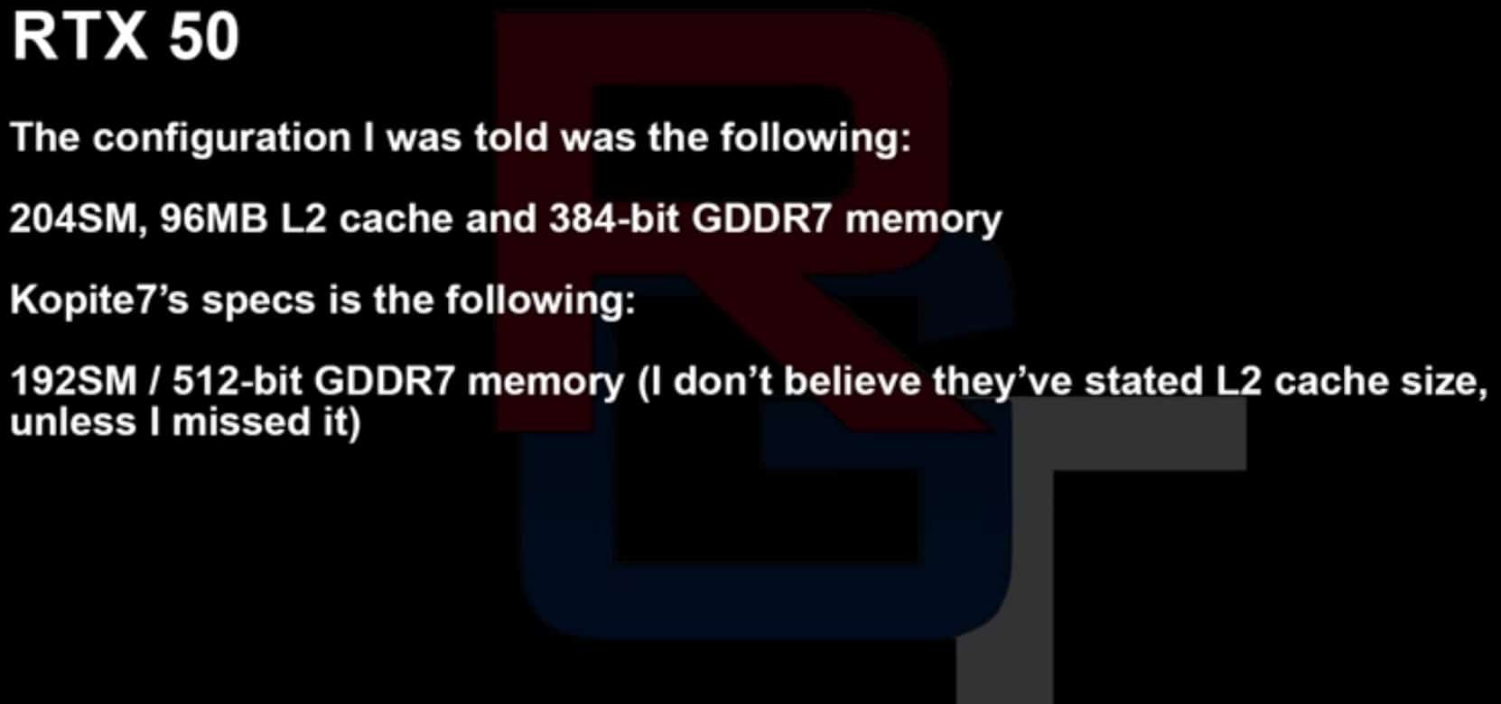
The GeForce RTX 5090 will be NVIDIA’s next gaming flagship, doubling down on memory, cache, and cores. Multiple sources have shared their findings on the Blackwell top gun, which we’ll discuss in this post. RedGamingTech claims that the RTX 5090 will feature 204 SMs for a total of 26,112 cores. On the memory side, we’re looking at 32Gbps GDDR7 memory paired with a 384-bit bus. The L2 cache will be consolidated to 96MB as well. Plans of using a 512-bit bus seem to have been shelved.
According to @kopite7kimi, the next-gen Blackwell “GB202” gaming die will have a 12 (GPCs) x 8 (TPCs) configuration. This would result in a massive GPU featuring 12 GPCs (Graphics Processing Clusters), each with 8 TPCs (Texture Processing Clusters). A TPC comprises 2 SMs (Streaming Multi-Processors), each of which contains 128 FP32 cores. The above numbers net a core count of 24,576 (192 SMs) for the fully enabled GB202 die. Like its predecessor, the GeForce RTX 5090 should contain a few disabled SMs to ensure proper yields. Optimistically, we can expect a core count of 24,046 or less.
The GeForce RTX 5090 with 32Gbps GDDR7 memory and a 384-bit bus would produce an external memory bandwidth of 1,536 GB/s, up from 1,008 GB/s on the RTX 4090. A 50% increase in memory throughput backed by a ~60% gain in shader density would easily net generational uplifts of up to 2x or more. It’s still too early to finalize a number, but it’d be fair to say that the RTX 5090 should deliver the same kind of upgrade as its predecessor.
Graphics Card Name
NVIDIA GeForce RTX 4090
NVIDIA GeForce RTX 4080
NVIDIA GeForce RTX 4070 Ti
NVIDIA GeForce RTX 4070
NVIDIA GeForce RTX 4060 Ti
NVIDIA GeForce RTX 4060
Die
AD102
AD103
AD104
AD104
AD106
AD107
FP32 Cores
16384
9728
7680
5888
4352
3072
TMUs/ROPs
512/176
320/112
240/80
184/64
136/48
TBD
Tensor/RT Cores
512/128
304/76
240/60
184/46
136/34
TBD
L2 Cache
72 MB
64 MB
48 MB
36 MB
32 MB
24 MB
Base Clock
2230 MHz
2210 MHz
2310 MHz
1920 MHz
2310 MHz
1830 MHz
Boost Clock
2520 MHz
2510 MHz
2610 MHz
2475 MHz
2535 MHz
2460 MHz
VRAM
24 GB GDDR6X
16 GB GDDR6X
12 GB GDDR6X
12 GB GDDR6X
8-16 GB GDDR6
8 GB GDDR6
Bus Width
384-bit
256-bit
192-bit
192-bit
128-bit
128-bit
Memory Clock
21.0 Gbps
23.0 Gbps
21.0 Gbps
21.0 Gbps
18.0 Gbps
17.0 Gbps
Bandwidth
1008 GB/s
736 GB/s
504 GB/s
504 GB/s
288 GB/s (554 GB/s Effective)
272 GB/s (453 GB/s Effective)
TBP
450W
320W
285W
200W
160/165W
115W
MSRP
$1599
$1199
$799
$599
$399-$499
$299
Launch
12th Oct 2022
16th Nov 2022
5th Jan 2023
13th April 2023
24th May/ Jul 2023
Jul 2023
An RTX 5080 featuring a bus width of 192-bit and 32Gbps GDDR7 memory would net bandwidth of 768GB/s, a small upgrade from the 717GB/s offered by the RTX 4080. Neither the RTX 4080 nor the 4080 Super utilize a 192-bit bus. With Ada, NVIDIA is using larger L2 cache buffers to improve on-die hit rates, and when they’re not being stingy with DRAM, it mostly works.
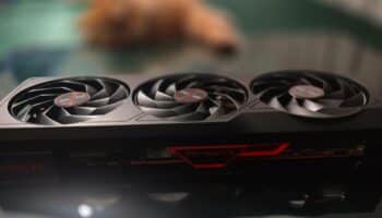
The GeForce RTX 5090 Founders Edition will allegedly use the same heatsink as the recently leaked RTX 4090 Ti. This massive thermal solution is four slots wide with four fans and a complex, side-mounted PCB. The final design will likely be toned down as there’s no need for such a large shroud.
We already know that the RTX 4090 runs well on cheap, aftermarket coolers. There’s no reason for the RTX 5090 to accommodate a similar-sized heatsink even though it’s expected to be fabbed on TSMC’s 3nm-class process technology.
Processors, PC gaming, and the past. I have written about computer hardware for over seven years with over 5000 published articles. I started during engineering college and haven't stopped since. On the side, I play RPGs like Baldur's Gate, Dragon Age, Mass Effect, Divinity, and Fallout. Contact: areejs12@hardwaretimes.com.