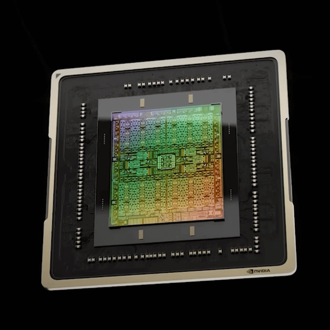
NVIDIA is allegedly going to leverage a chiplet design for its next-gen Blackwell GPUs. According to @kopite7kimi, GB100, the successor to the H100 “Hopper” data center GPU, will use a multi-chip module (MCM) architecture. After exceeding a die area of 800mm² and 80,000 million transistors, NVIDIA will look to advanced packaging technologies such as TSMC’s CoWoS to increase the IC count, following AMD’s Navi 3X and MI300 designs.
As per @AGF, the top-end Blackwell gaming GPU will leverage a “GB101” chiplet to power the RTX 5090 or the 5090 Ti or perhaps even the next-gen Titan SKU. The entire Blackwell family is said to be fabbed on TSMC’s N3 (3nm) class process node, promising the highest level of transistor density and power efficiency.
The Blackwell graphics architecture will make significant changes to the individual processing units such as the GPC (Graphics Processing Cluster), TPC (Texture Processing Cluster), and SM (Streaming Multi-Processor). We can also expect notable changes to the bus to accommodate a disaggregated design. As far as the GeForce RTX consumer GPUs are concerned, only the top-end SKUs, such as the RTX 5090, 5090 Ti, and/or RTX Titan, will leverage MCM. The lower-end SKUs will remain monolithic.


