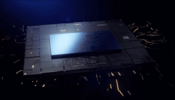
NVIDIA launched its next-gen data center graphics card the other day in the form of the H100 (GH100), giving us a first look at the Hopper architecture. Leveraging TSMC’s N4 4nm process node on a massive die, it doubles down on Ampere’s compute capabilities. From what we’ve heard about the GeForce RTX 4080/4090 (Ada Lovelace), it’d be fair to say that the AD102 will be a derivative of the GH100.
| Data Center GPU | NVIDIA Tesla P100 | NVIDIA Tesla V100 | NVIDIA A100 | NVIDIA H100 |
|---|---|---|---|---|
| GPU Codename | GP100 | GV100 | GA100 | GH100 |
| GPU Architecture | NVIDIA Pascal | NVIDIA Volta | NVIDIA Ampere | NVIDIA Hopper |
| SMs | 56 | 80 | 108 | 132 |
| TPCs | 28 | 40 | 54 | 66 |
| FP32 Cores / SM | 64 | 64 | 64 | 128 |
| FP32 Cores / GPU | 3584 | 5120 | 6912 | 16896 |
| FP64 Cores / SM | 32 | 32 | 32 | 32 |
| FP64 Cores / GPU | 1792 | 2560 | 3456 | 8448 |
| INT32 Cores / SM | NA | 64 | 64 | 64 |
| INT32 Cores / GPU | NA | 5120 | 6912 | 8448 |
| Tensor Cores / SM | NA | 8 | 42 | 4 |
| Tensor Cores / GPU | NA | 640 | 432 | 528 |
| Texture Units | 224 | 320 | 432 | 528 |
| Memory Interface | 4096-bit HBM2 | 4096-bit HBM2 | 5120-bit HBM2 | 512-bit x5 |
| Memory Size | 16 GB | 32 GB / 16 GB | 40 GB | 128GB? |
| Memory Data Rate | 703 MHz DDR | 877.5 MHz DDR | 1215 MHz DDR | 1600 MHz DDR? |
| Memory Bandwidth | 720 GB/sec | 900 GB/sec | 1555 GB/sec | ? |
| L2 Cache Size | 4096 KB | 6144 KB | 40960 KB | 60MB |
| TDP | 300 Watts | 300 Watts | 400 Watts | 700W |
| TSMC Manufacturing Process | 16 nm FinFET+ | 12 nm FFN | 7 nm N7 | 4 nm N4 |
Both feature a maximum of 144 SMs or 18,432 cores across 12 GPCs and 72 TPCs. The IN32: FP32 cores exist in a 1:2 ratio per SM, much like Ampere (with the FP64 cores disabled on Ada). The only tangible differences are with respect to the L2 cache and the memory controllers. Lovelace should feature GDDR6X/GDDR7 controllers while Hopper uses HBM2e. The former is expected to pack up to 96MB of L2 cache while the latter is limited to 60MB.
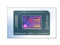
Other than that, the two graphics architectures have the same floorplan, and it won’t be surprising if NVIDIA uses the N4 node for the AD102 as well. Looking at NVIDIA’s spending on foundry costs over the past months, it’s looking more and more likely that Lovelace will be an N4 die. Either way, the PPA difference between N5 and N4 is minimal at best, and shouldn’t affect the final product or performance.
| GPU | TU102 | GA102 | AD102 | AD103 | AD104 |
|---|---|---|---|---|---|
| Arch | Turing | Ampere | Ada Lovelace | Ada Lovelace | Ada Lovelace |
| Process | TSMC 12nm | Sam 8nm LPP | TSMC 5nm | TSMC 5nm | TSMC 5nm/ 4nm |
| GPC | 6 | 7 | 12 | 7 | 5 |
| TPC | 36 | 42 | 72 | 42 | 30 |
| SMs | 72 | 84 | 144 | 84 | 60 |
| Shaders | 4,608 | 10,752 | 18,432 | 10,752 | 7,680 |
| TP | 16.1 | 37.6 | ~90 TFLOPs? | ~50 TFLOPs | ~35 TFLOPs |
| Memory | 11GB GDDR6 | 24GB GDDR6X | 24GB GDDR6X | 16GB GDDR6 | 16GB GDDR6 |
| L2 Cache | 6MB | 6MB | 96MB | 64MB | 48MB |
| Bus Width | 384-bit | 384-bit | 384-bit | 256-bit | 192-bit |
| TGP | 250W | 350W | 600W? | 350W? | 250W? |
| Launch | Sep 2018 | Sep 2020 | Aug-Sep 2022 | Q4 2022 | Q4 2022 |
Then, there’s the matter of power consumption. There have been several rumors claiming that NVIDIA’s next-gen RTX 4080/4090 graphics cards will have an abysmal power consumption of up to 700-800W. As already stated in earlier posts, this is highly unlikely and the TBP of the Ada Lovelace GPUs should top out at 600W, with only extreme overclocker cards such as the RTX 4090 Kingpin coming close to this limit. Toms from MLID has gotten similar hints from his sources: