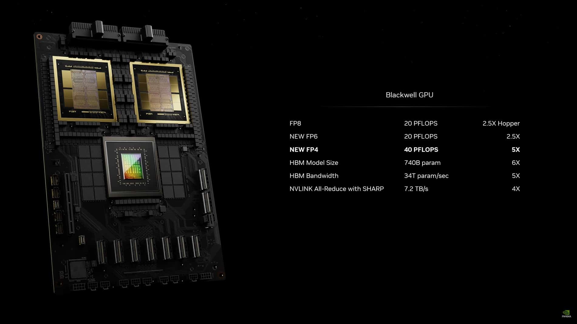
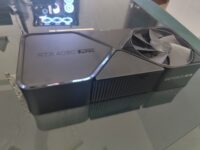
Update: NVIDIA has officially launched the first Blackwell GPU, the B200. It features a modular design with two GPU dies fabbed on the 4nm (TSMC N4) node. The dual-chip package consists of 192GB HBM3e memory paired using eight 1024-bit memory controllers (8,192-bit overall), offering 8 TB/s memory bandwidth. The B200 consists of 8 HBM stacks, each consisting of 24GB “8-Hi” memory packages. The GPU has a peak TBP of 700W.
Being relevant to network training, NVIDIA is focusing on low-precision compute for Blackwell. FP8 performance is 2.5x higher than Hopper at 20 PFLOPS. FP16/BF16 throughput is capped at 5 PFLOPS and TF32 peaks at 2.5 PFLOPS. Including sparsity, these represent a 2.5x uplift over Hopper.
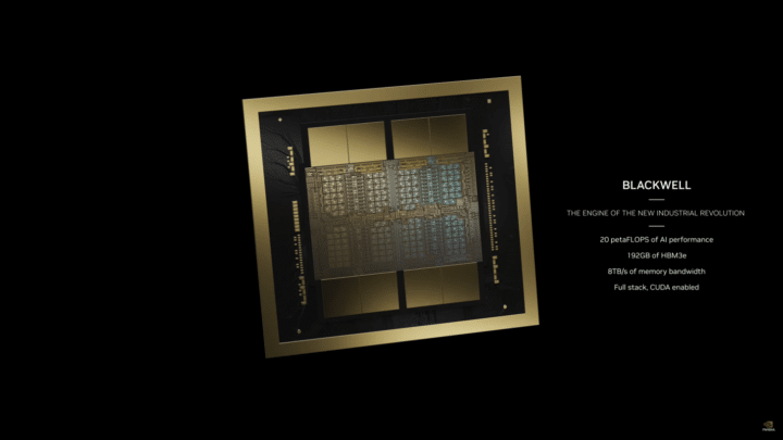
The 2nd Gen Transformer Engine on Blackwell automatically converts language models to the necessary format for optimal performance. To aid it, a new FP6 format has been included that acts as the placeholder where FP4 is insufficient and FP8 is excessive.
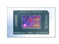
Some of the key specifications of NVIDIA’s Blackwell Tensor core GPUs have leaked out. According to @XpeaGPU, the B100 will feature two dies packaged using CoWoS-L, making it the first modular (chiplet-based) NVIDIA GPU. The GPU will be surrounded by 8 HBM3e stacks (8-Hi), offering 192GB of high-bandwidth memory. Its predecessor, the H100, offers 80GB HBM3 memory spread across 5 stacks using 10 512-bit memory controllers each. I reckon the B100 will utilize 12 to 13 512-bit memory controllers to connect the 8 HBM3e stacks.

The B200, scheduled to launch next year, will allegedly increase the graphics memory to 288GB using 12-Hi HBM3e stacks. The memory bus and number of HBM packages should remain unchanged at 13x 512-bit and 8, respectively. Not much info is provided on the GPU (cores, SMs, GPCs). The use of CoWoS-L for two graphics dies implies a massive increase in shader density. I think a GPC count of 10-12 would be reasonable.
A B100 with 12 GPCs would feature over 27K FP32 cores and 864 Tensor cores. The H100 consists of 16,896 FP32 cores and 528 Tensor cores. It will be interesting to see if the SMs or GPCs are modified, but the rest shouldn’t change much. The B100 is expected to be unveiled by the company CEO later today during the GTC 2024 keynote.