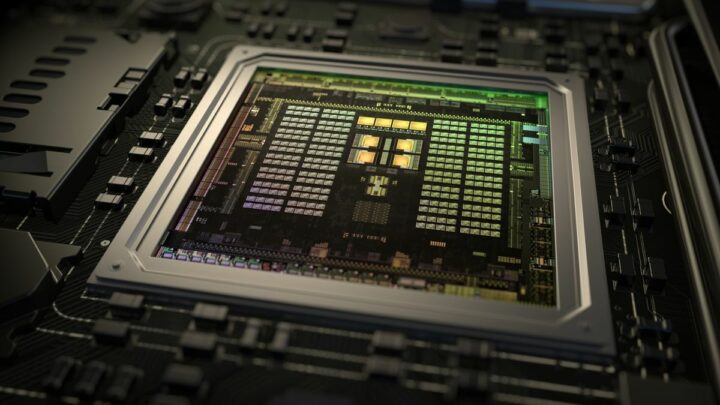
Nintendo passed on an Ada Lovelace-based SoC (RTX 40), opting instead for a four-year-old design for the Switch 2. According to “Moore’s Law is Dead,” NVIDIA first offered Nintendo a chip based on the Lovelace graphics architecture which powers the RTX 40 series GPUs (and supports DLSS 3 FG). However, it was rejected for an older, much cheaper SoC based on the Ampere graphics architecture (launched in May 2020).
Profit margins are the reason why Nintendo rejected Ada Lovelace. The RTX 40 series GPUs fabbed on TSMC’s cutting edge 5nm node are highly efficient but pricey. A Switch 2 SoC with similar properties would significantly reduce Nintendo’s profit margins. On the other hand, the Tegra T239 which leverages the Ampere architecture relies on Samsung’s 8nm LPP process. This node is a variant of the foundry’s 10nm process, comparable to TSMC’s 7nm process from 2016-17.
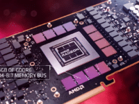

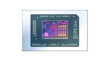
A node as old as the 8LPP will cost a fraction of what NVIDIA pays for N5. The T239 features an octa-core Arm A78C CPU and an Ampere GPU with 1,535 cores. The SoC has a 128-bit memory controller which when paired with LPDDR5 memory offers a peak bandwidth of 102GB/s.
The Switch 2 should be faster than the Steam Deck but barely ahead of the ROG Ally or the Legion GO. Nonetheless, considering Nintendo’s suite of games (mostly 2.5D), the T239 should be sufficient. NVIDIA’s DLSS 2 upscaling will provide the required future-proofing.
Further reading: