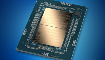
Intel shared its ambitious plan to retake process leadership from its Asian rivals during its Investor keynote the other day. Team Blue plans to launch its first chiplet (tiled) architecture with Meteor Lake in 2023. Fabbed on the Intel 4 process node, it’ll mix and match different process nodes across four different tiles on the same substrate. While the CPU tile featuring the performance, and efficiency core cluster will almost certainly be fabbed on Intel’s internal 4nm node, the GPU tile will be fabbed on TSMC’s 3nm node. The SoC or the IO tile won’t be outsourced as the N3 node is too expensive for those. That leaves us with the graphics tile.
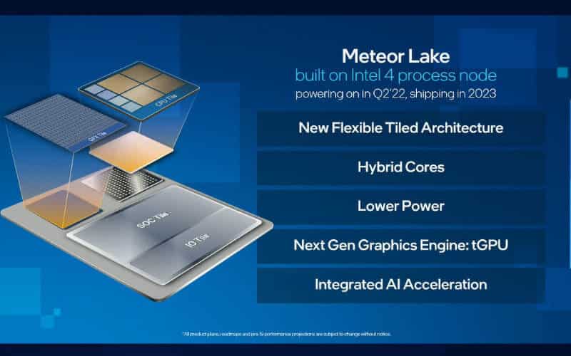
Going by the above block diagram, it would also seem that the performance core count is being increased to at least 8 (if not 16) on the mobile platform, with the efficiency core cluster growing to 16 for a total of 20-32 cores, and 48 threads.


For Arrow Lake, the core count will definitely be increased to 32 (8P + 8E), and the thread count to 48. The 3nm graphics die will offer ample visual performance for the desktop market while also keeping costs in check.
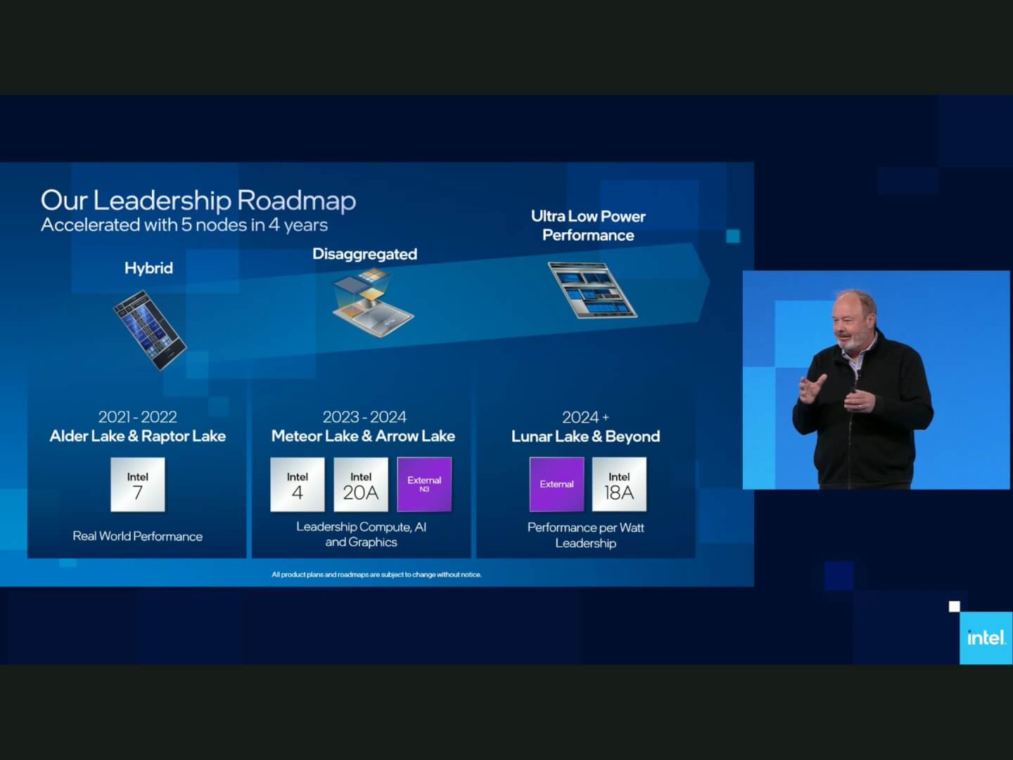
Overall, looking at Intel’s updated roadmap, it seems that the chipmaker will be on par with TSMC (and AMD) at least in terms of process technology by 2024. Combined with advanced packaging technologies such as Foveros and EMIB, the 20A (2nm) and the 18A (1.8nm) process nodes should allow Team Blue to catch up with its East Asian peers, if not outright beat them.