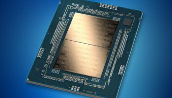
Intel has reaffirmed its foundry roadmap, squashing rumors of next-gen CPU architecture and process delays. The latest update comes from IEEE, highlighting the chipmaker’s plans to regain process leadership by the end of 2024. Currently, the bulk of Intel’s CPU families is fabbed on the 7nm node (formerly 10nm ESF). These include 12th Gen Alder Lake, 13th Gen Raptor Lake, and the 4th Gen Xeon Scalable “Sapphire Rapids” processors.
The Intel 4 process (previously 7nm) is already manufacturing-ready, with risk production underway. Mass production should commence in early 2023, so the 14th Gen Meteor Lake processors should launch in the second half of 2023. Or, at the very least, the mobility lineup should. It will bring a 20% improvement in performance per watt and feature the first implementation of EUV lithography.


The Intel 3 process is designed exclusively for the data center, namely Granite Rapids and Sierra Forest. The former will feature up to 128 P-cores (Redwood Cove?) across three compute tiles, while the latter will be a cloud-centric architecture with up to 256 cores.
The 20A process (2nm) node will be the defining moment in Intel’s foundry history. Bringing an additional 15% improvement per watt in performance, it’ll leverage RibbonFET and PowerVia technologies. RibbonFET is Intel’s version of GAA (Gate All Around) transistors set to succeed FinFET after nearly a decade. PowerVia is a backside power delivery scheme power delivery system meant to improve efficiency further.
A traditional interconnect technology sits on top of the transistor layer with all the power and signal wires integrated (Figure 1a). This intermingling of power and signal wires creates a bottleneck in terms of space but also opens the door to a host of interference, signal coupling, and power integrity issues. Ideally, signal and power lines would be completely separated.
With PowerVia, this separation is achieved. The power wires are placed underneath the transistor layer, on the backside of the wafer (Figure 1b). Power is delivered directly from the package to the transistors through a network of metal layers that are optimized for power delivery with features such as maximum metal volume for low resistance (lower losses) and good grounding (ensures power integrity)
Intel
The 20A process will be the foundation of the desktop-centric Arrow Lake processors. Risk production is planned for early 2024, and volume manufacturing later the same year. This will be when Intel overtakes TSMC or, at the very least, stand on equal footing in manufacturing prowess. TSMC’s 3nm process is already in mass production, with an enhanced variant planned for 2024. Its 2nm process utilizing GAA technology won’t begin volume production anytime before 2025.
On the other hand, Intel claims that its 18A (1.8nm) process is on track for risk production in late 2024, with mass production set to begin in 2025. It will offer a 10% performance per watt improvement, an enhanced variant of RibbonFET, and support for advanced interconnect technologies.
Via: IEEE