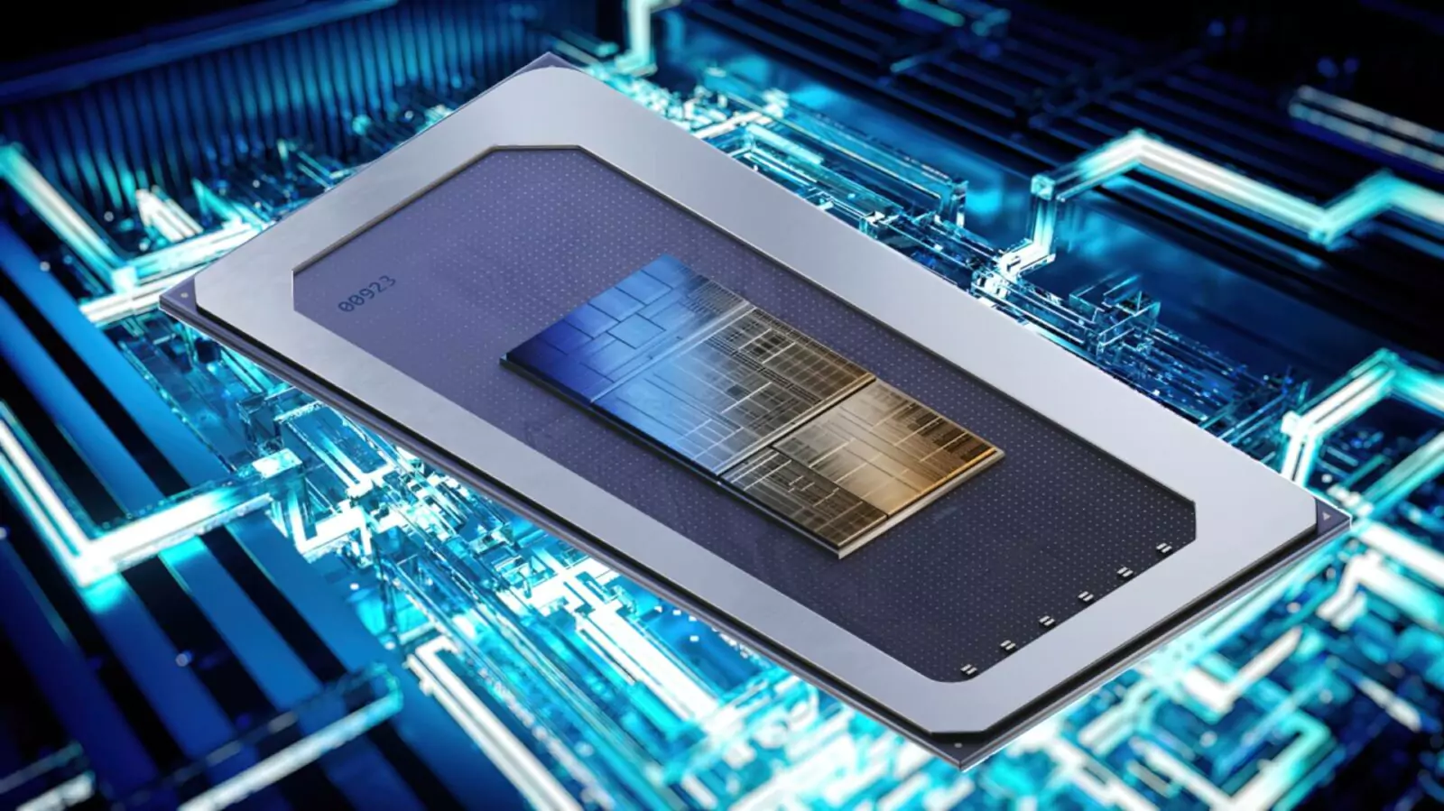
The 1st Gen Core Ultra Meteor Lake processors represent the most significant upgrade for Intel’s client portfolio since Alder Lake. At least on paper. It features upgraded core architectures and a 4nm-class process node. It is also the first chiplet-based design from Team Blue. However, according to Tim Wilson, the VP of Intel’s Engineering Group and GM of SoC design, the Meteor Lake cores are largely identical to the preceding 13th Gen Raptor Lake family.

Intel’s 1st Gen Core Ultra processors are the first to benefit from three differently optimized core architectures. You’ve got the Redwood Cove “P” cores, Crestmont “E” cores, and another pair of Crestmont “LPE” cores. Wilson revealed that Redwood Cove and Crestmont cores are architecturally similar to the Raptor Cove and Gracemont cores powering Raptor Lake.


Comparing the block diagrams of the two pairs of core architectures, most of the last-gen design has been retained apart from minor changes. The Crestmont core has a slightly wider Allocate/Rename Buffer with some tweaks to the Vector Execution Units.
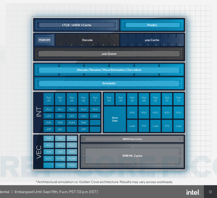
The Redwood Cove core is almost exactly like Golden Cove. The same decoders, allocation Q, and op-cache are paired with an identical memory subsystem. The Vector EUs get a new AMX unit for matrix workloads, but this may or may not come to the client platform. Like the AVX512 unit, it may be reserved for the data center offerings.
As is the tradition with node shrinks, the Reorder Buffer should get bigger with minor changes to the scheduler, registers, and branch predictor.

Tim explains that Meteor Lake, a major node upgrade (Intel 7->Intel 4), brings considerable improvements to power efficiency (does it though?). With the Core Ultra processors, Intel’s engineers focused on software/firmware optimizations to achieve a stable process flow. This is the Tick Tock model all over again. A node shrinks (tick), followed by a microarchitectural update (tock).
Tim clarified the differences (or rather the lack thereof) between the E-cores on the compute die and the LPE cores on the SoC die. It turns out that they share the same microarchitecture but are optimized for different workloads. The E-cores on the compute die have been fine-tuned for higher performance and multi-threaded workloads, while the LPE cores on the SoC die are optimized for lightly threaded low-power tasks.
Unfortunately for Intel, the Core Ultra processors aren’t power efficient either. They lose to AMD’s year-old Ryzen 7000 “Phoenix” chips in most scenarios while also being slower. A recent firmware update improved performance and efficiency, but how many updates will Meteor Lake need to become competitive?

Can you explain to me how different the P-core and E-cores of Meteor Lake are compared to Raptor Lake?
Tim: Compared to the previous generation of Raptor Lake, the microarchitecture of both the P and E cores in Meteor Lake has some improvements. However, we introduced Meteor Lake with the new Intel 4 process. In general, when we introduce new processes, we tend to reduce the risk in terms of architecture. Once we achieve a stable process flow, we tend to make a bigger leap by improving the architecture. So, since this is a new big node update for us, and we can also get the energy efficiency benefits of Intel 4, we’ve made very few changes to the core architecture, so they’re architecturally very similar to Raptor Lake’s E-cores and P-cores.
Can you tell us more about the technical differences between traditional E-cores and low-power E-cores?
Tim: First, in Meteor Lake, the E cores in the compute module and the LPE cores in the SoC block have the same architecture. But the difference is that we optimize them differently for different tasks. The E-cores in the compute block are optimized for higher performance and multithreaded tasks, while the LPE cores in the SoC block are optimized for tasks that are low-power and do not require the full computing power of the P/E cores in the compute block. So, from an architectural point of view, they are the same, but again from an optimization and performance per watt point of view.
The I/O module is built with TSMC N6, is it a technical problem or a cost issue?
Tim: I would say that as an engineer, the most interesting problems to solve are technical problems, and the (most) boring are the cost problems and similar problems that we have to solve. Of course, at some point this must also be taken into account. As you said, IO modules based on TSMC N6 require high-voltage type transistors using a more mature and stable process, and many types of chips have proven to be able to use this process. We can take advantage of this effectively and at a lower cost.
Then we already have the base module, which as an intermediate needs to fuse other modules. What process is it made of?
Tim: This is an Intel node, we call it the 1227 node, and you may not remember the name because it is not a widely known node. As you said, this is a passive exchanger, that is, there are no active devices on this node. What it does is basically provide “wires” between the blocks placed on it and serve as a base through miniature connectors.