A while back, NVIDIA announced its GeForce RTX 2050, MX550 and MX570 mobile GPUs. Two of these SKUs are based on the Ampere microarchitecture, with the RTX 2050 and the MX570 leveraging the GA107 core, and the MX550 being a derivative of the Turing-class TU117 core. The MX550 features around 1,024 shaders paired with 4GB of GDDR6 memory, while the MX570 will likely increase that figure to 1,280-1,536 (Ampere) FP32 cores.
| MX570 | MX550 | |
| CUDA Cores | 1024+ | 1024? |
| ROPs | 32? | 32? |
| Memory Clock | 12Gbps GDDR6? | 12Gbps GDDR6? |
| Memory Bus Width | 64-bit | 64-bit |
| TDP Range | 30W? | 30W? |
| GPU | GA107 | TU117 |
| Architecture | Ampere | Turing |
| Launch Date | Spring 2022 | Spring 2022 |
| RTX 3060 Laptop GPU | RTX 3050 Ti Laptop GPU | RTX 3050 Laptop GPU | RTX 2050 Laptop GPU | |
| CUDA Cores | 3840 | 2560 | 2048 | 2048 |
| ROPs | 48 | 32 | 32 | 32? |
| Boost Clock | 1283 – 1703MHz | 1035 – 1695MHz | 1057 – 1740MHz | 1155 – 1477MHz |
| Memory Clock | 14Gbps GDDR6 | 14Gbps GDDR6 | 14Gbps GDDR6 | 14Gbps GDDR6 |
| Memory Bus Width | 192-bit | 128-bit | 128-bit | 64-bit |
| VRAM | 6GB | 4GB | 4GB | 4GB |
| TDP Range | 60 – 115W | 35 – 80W | 35 – 80W | 30 – 45W |
| GPU | GA106 | GA107 | GA107 | GA107 |
| Architecture | Ampere | Ampere | Ampere | Ampere |
| Manufacturing Process | Samsung 8nm | Samsung 8nm | Samsung 8nm | Samsung 8nm |
| Launch Date | 01/26/2021 | 05/11/2021 | 05/11/2021 | Spring 2022 |
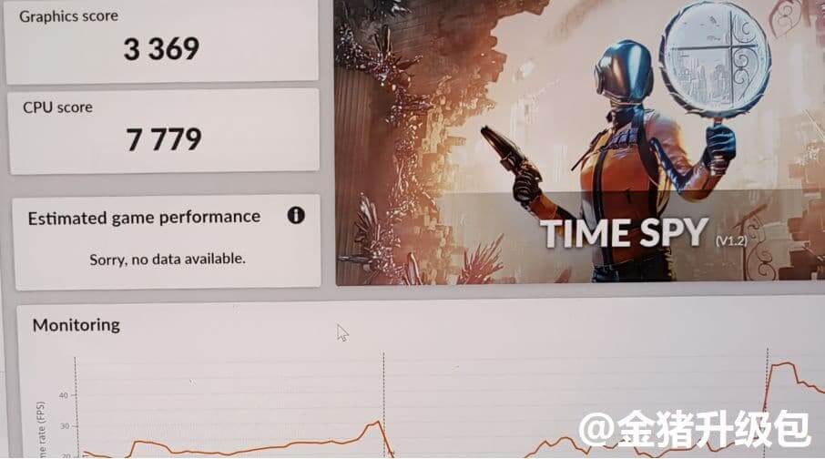
The RTX 2050, despite using the Turing nomenclature is based on the Ampere design, packing 2,048 FP32 cores and 4GB of GDDR6 memory via a 64-bit bus. Thus, we’re essentially looking at the 3050 with a slimmer bus. Two 3DMark Time Spy results of the RTX 2050 and MX550 have surfaced. The RTX 2050 scores 3,369 points in TimeSpy while the MX550 is limited to just 2,510.

In comparison purposes, a recently leaked Rembrandt score shows AMD’s next-gen RDNA 2 integrated graphics scoring over 2,700 points, easily outmaneuvering the MX550. This is rather disappointing as this SKU will launch alongside Rembrandt in early 2022, and being a discrete GPU should be at least 15-20% faster than AMD’s integrated graphics solutions. We’ll probably see situations where OEMs pair these two in one design, making the dGPU redundant, and a sheer waste of silicon.
Via: Hardware