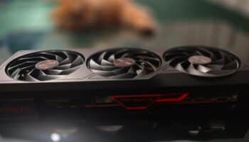
AMD plans on launching its first modular gaming GPUs later this year. Based on the RDNA 3 graphics architecture and TSMC’s N5/N6 process nodes, the Radeon RX 7000 graphics cards are expected to bring unprecedented performance gains for gamers at every price point. We’re talking about (at least) 2x levels of sheer raster and even higher ray-tracing uplifts across most popular titles.
The Radeon RX 7900 XT at the very top will reportedly consist of two GCDs (Graphics Compute Dies) with a bridge interconnect 3D stacked on top of the two along with 256MB of L3/Infinity Cache. It will pack up to a total of 15,360 shaders across 60 Work Group Processors (WGPs) paired with 16GB of GDDR6 memory across a 256-but bus. The GPU core will run at around 2.5GHz, the same as Navi 21 which is likely a result of the densely packed logic. Overall, the Navi 31 die powering the Radeon RX 7900 XT should be 2.2-2.5x faster than its predecessor, with the RX 7800 XT beating the RX 6800 XT by 70-80%.

However, much like the GeForce RTX 40 series lineup, it’s the mid and upper midrange offerings that will be more compelling. In NVIDIA’s case, the AD103 die powering the GeForce RTX 4070/4060 Ti is set to be 10-30% faster than the RTX 3090 in traditional raster performance and 40-50% faster in ray-tracing workloads like RTGI, RTR, RTAO, RTS, etc. As for the RTX 4060 (AD104), we’re looking at RTX 3080 levels of generalized raster and impressively, RTX 3090 Ti levels of ray-tracing performance.
AMD is looking to offer similar levels of graphics performance to the mainstream gamer. The Radeon RX 7700 XT (Navi 33) is reportedly going to be faster than the Radeon RX 6900 XT when clocked at 2.8GHz. This results in an FP32 throughput of over 23 TFLOPs with a modest 220-250W power draw. There’s very scarce information on RDNA 3’s ray-tracing capabilities, but expect them to be at least comparable to Ada.
Previous coverage on the Radeon RX 7000 GPUs:
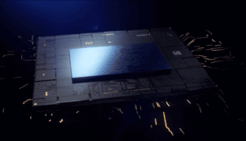
A mockup of the Navi 3x design can be seen below:
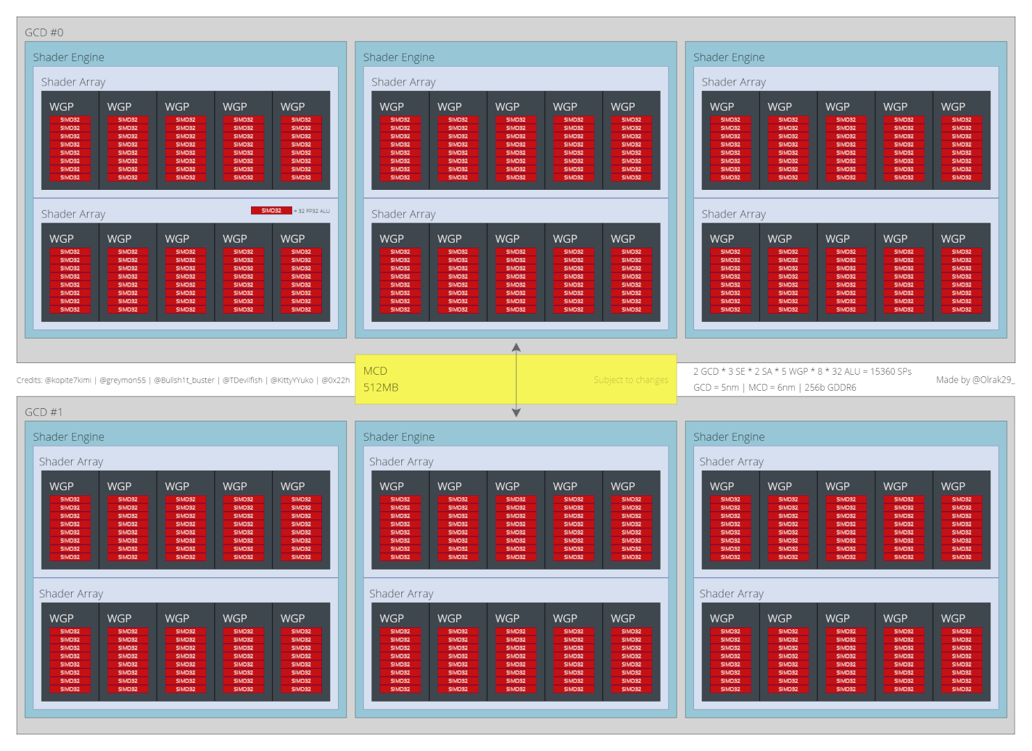
Each Graphics Die (GCD) features three Shader Engines which are made up of two Shader Arrays each. In turn, each Shader Array packs five WGPs containing eight SIMD units (vs four on RDNA 2). The two dies are connected by a bridge interconnect paired with 256MB of L3 “Infinity” Cache. According to the source, the GCDs will be fabbed on TSMC’s 5nm (N5) node while the MCD will be fabbed on the older 6nm (N6) node. Each die should come with a 128-bit bus (divided into eight controllers), resulting in an overall bus width of 256-bit and the same external bandwidth of 448GB/s as the RX 6800 XT/6900XT.
AMD’s RDNA 3 graphics architecture is expected to get a major overhaul at the front-end, with redesigned Work Group Processors in place of Compute Units, or Dual Compute Units. With RDNA 1 and 2, the WGPs were the basic units for workload scheduling (from CUs on GCN/Vega), but it looks like that is going to change again with Navi 3x. Dual Compute Units are being discarded in favor of wider Work Group Processors, packing as many as 256 stream processors across eight 32-wide SIMDs. This means that the wave32 format of scheduling will be retained, but the number of overall active waves will be increased.