AMD’s Navi and NVIDIA’s Turing (used to) power the latest GPUs from Teams Red and Green, respectively, The Radeon Navi cards are based on the RDNA architecture which is a complete reimagining of AMD’s approach to gaming GPUs with low latencies and high clocks. NVIDIA’s RTX 20 series “Turing” GPUs, on the other hand, aren’t that different from the preceding Pascal GPUs in terms of design, but they do add a couple of new components crucial for “Tur(n)ing RTX On”.
In this post, we compare the latest NVIDIA and AMD GPU architectures namely Turing and Navi:
Navi 10 is codename of the GPUs based on the RDNA uarch while TU102 is the codename of the GPUs based on the Turing uarch.
AMD Navi vs NVIDIA Turing : Introduction
In simple terms, both NVIDIA and AMD’s GPU architectures consist of the same components which perform more or less the same operations. You’ve got the GPU containing execution units, fed by the schedulers and dispatchers. Then there is the cache memory connecting the GPU to the graphics memory and post-processing units, Texture Units, Render Output Units and Rasterizers performing the last set of operations before sending the data to the display.
If you magnify the above image and have a closer look at the execution units, the cache hierarchy, and the graphics pipelines, that’s where everything becomes complicated:
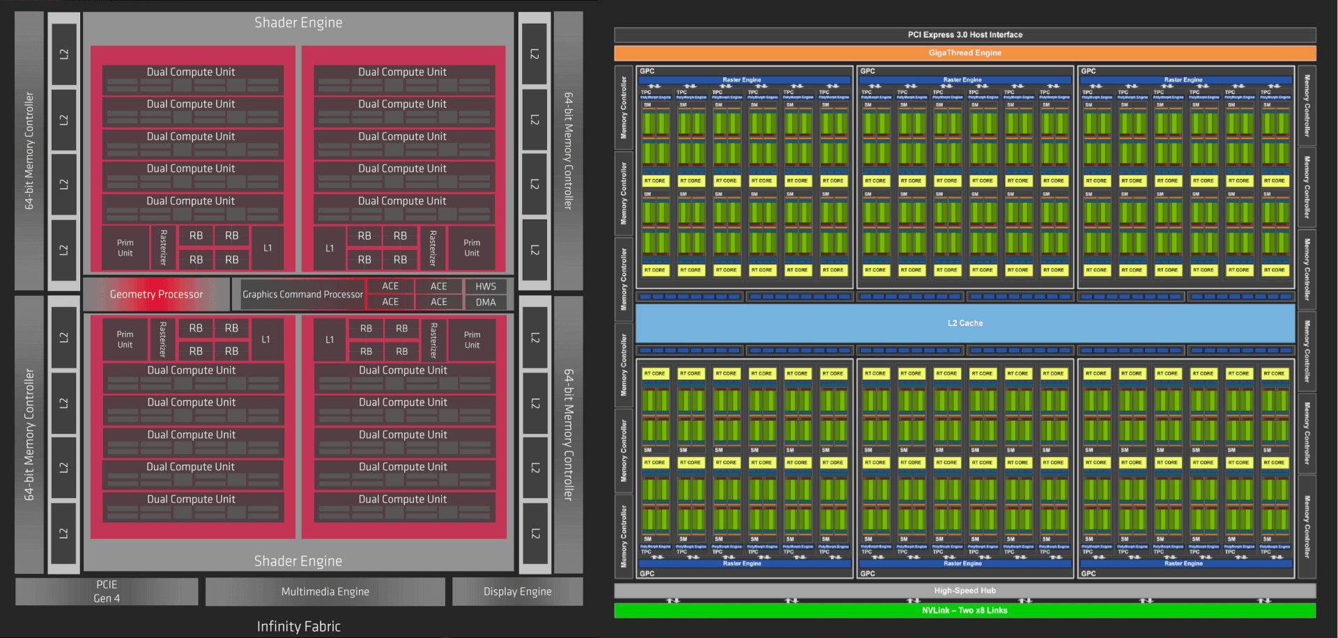
AMD Navi vs NVIDIA Turing GPU Architectures: SM vs CU
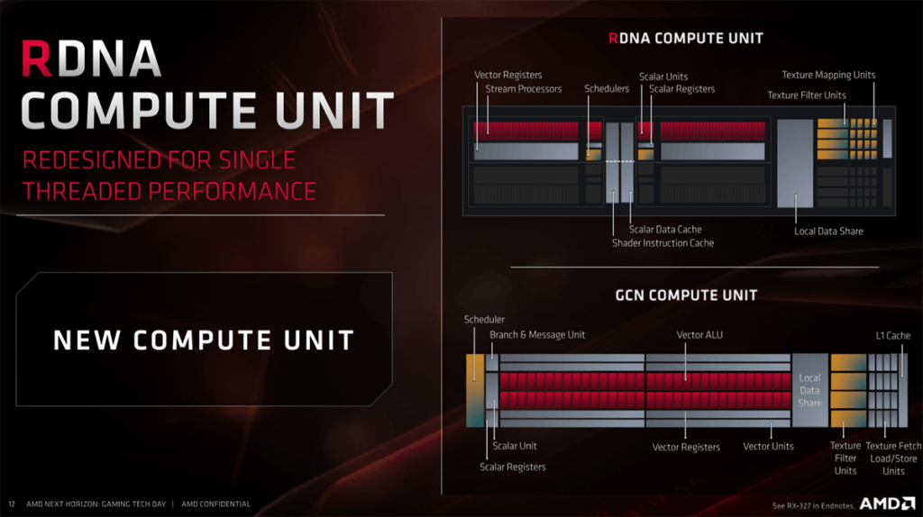
One of the main differences between NVIDIA and AMD’s GPU architectures is with respect to the cores/shaders and Compute Units (NVIDIA calls it SM or Streaming Multiprocessor). NVIDIA’s shaders (execution units) are called CUDA cores while AMD uses stream processors.
CUDA Cores vs Stream Processors: Super-scalar & Vector
AMD’s GPUs are vector-based processors while NVIDIA’s architecture is super-scalar in nature. While in theory, the former leverages the SIMD execution model and the latter relies on SIMT, the practical differences are few. In an AMD SIMD, there will always be room for 32 work items regardless of how many threads are executed per cycle. There might be 12, 15, 20, 25, or 30 threads being issued by an application per cycle, but the model supports 32 at a native level. Overall, the work is issued per CU in the form of waves, each containing 32 items.
What is SIMD? How Does it Work and How is it Different from SIMT?
With an NVIDIA SM, unless there’s no more work left, all the 128 work-queues (32 threads x 4) will always be saturated no matter which application is being used. Here the threads are independent of one another and can yield or converge with threads from other SMs as needed. This is one of the primary advantages of using a super-scalar architecture. The level of parallelism is retained and the utilization is also better.
One NVIDIA Turing SM has FP32 cores, INT32, and two tensor cores. There’s also the load/store, Special function unit, the warp scheduler, and dispatch. Like Volta, it takes two cycles to execute instructions (one INT and one FP). There are separate cores for INT and FP compute, and they work in tandem. As such, NVIDIA’s Turing SMs can execute both floating-point and integer instructions per cycle. This is NVIDIA’s implementation of Asynchronous Compute. While it’s not exactly the same thing, the purpose of both technologies is to improve GPU utilization.
AMD’s Dual CUs, on the other hand, consist of four SIMDs, each containing 32 shaders or execution lanes. There are no separate shaders for INT or FP, and as a result, the Navi stream processors can run either FP or INT per cycle. However, unlike the older GCN design, the execution happens every cycle, greatly increasing the throughput.
The reason behind this is that most games have short dispatches which weren’t able to fill the 4x 64 item queue of the GCN based Vega and Polaris GPUs. Furthermore, the four clock cycle execution made it even worse. With Navi, the one clock cycle execution greatly reduces this bottleneck, thereby increasing IPC by nearly 4x in some cases, putting the design efficiency on par with NVIDIA’s contemporary designs.
Turing vs Navi: Graphics and Compute Pipeline
In AMD’s Navi architecture, the Graphics Command Processor takes care of the standard graphics pipeline (rendering, pixel, vertex, and hull shaders) and the ACE (Asynchronous Compute Engine) issues Compute tasks via separate pipelines. These work along with the HWS (Hardware Schedulers) and the DMA (Direct Memory Access) to allow concurrent execution of compute and graphics workloads. Furthermore, there’s the geometry processor. It resolves complex geometry workloads including tessellation.
In Turing, the warp scheduler on an SM level and the Gigathread engine on the GPU level manage both Compute and graphics workloads. While concurrent compute isn’t the same as Async Compute, it functions similarly, with support for concurrent floating-point (mainly graphics) and integer (mainly compute) workloads.
Of Warps and Waves
In the case of AMD’s Navi, the workload items are issued in the form of a group of threads called waves. Each wave includes 32 threads (one for each shader in the SIMD), either compute or graphics and are sent to Dual Compute Units for execution. Since each CU has two SIMDs, it can handle two waves while a Dual Compute Unit can process four.
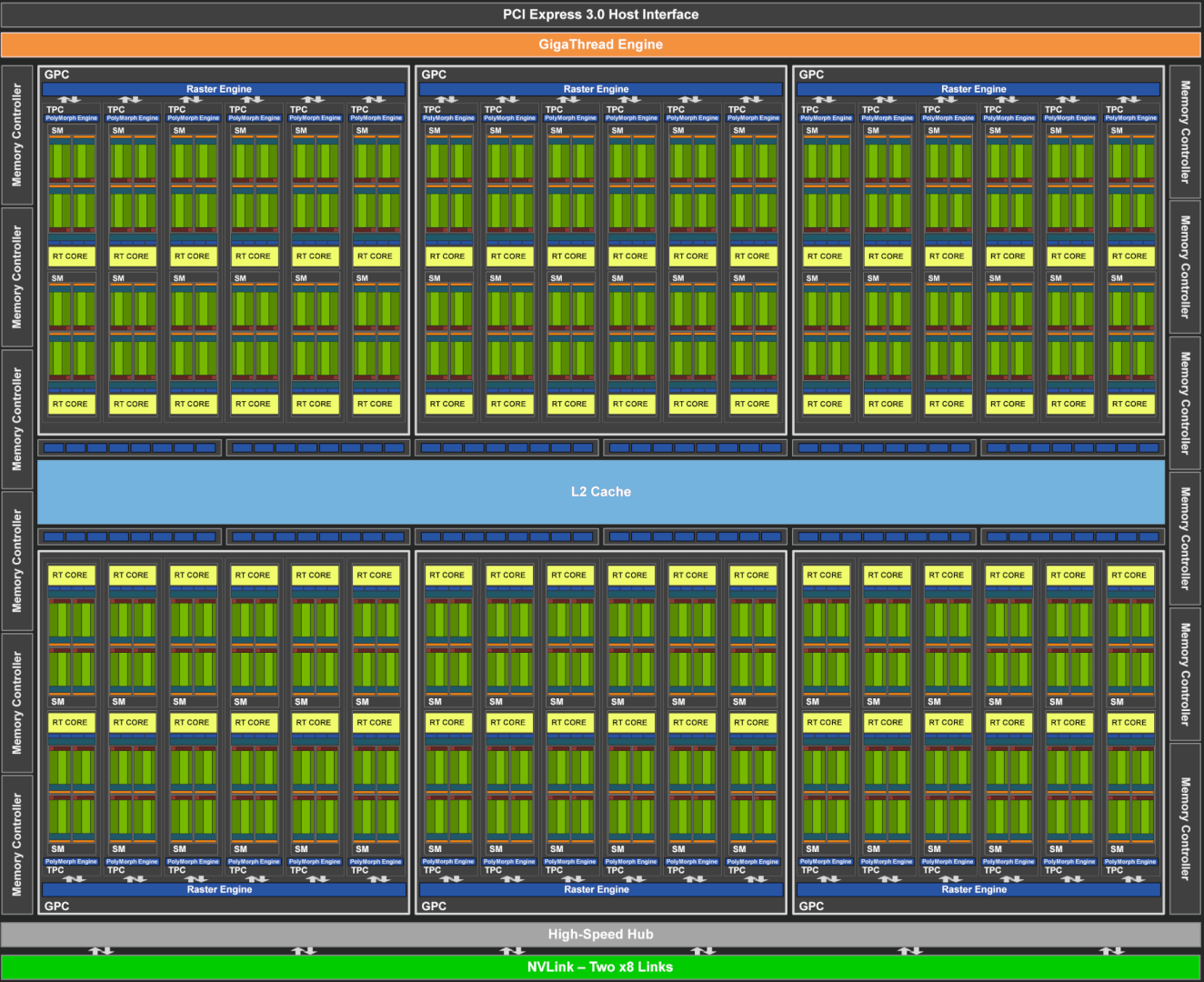
In NVIDIA’s case, the Gigathread Engine with the help of the Warp Schedulers manages thread scheduling. Each collection of 32 threads is called a warp. Each core (INT or FP) in an SM handles a warp. The threads in a warp originally didn’t on their own, but rather collectively. As such, a core could switch between different the warps available if there’s a stall.
Each thread doesn’t have a program counter, but a warp does. However, with Turing and Volta (and of course, Ampere), NVIDIA claims that each thread is independent and convergence is handled similar to Volta. Similar warp threads are grouped together into SIMT units and can yield or reconverge.
Green vs Red: Cache Hierarchy
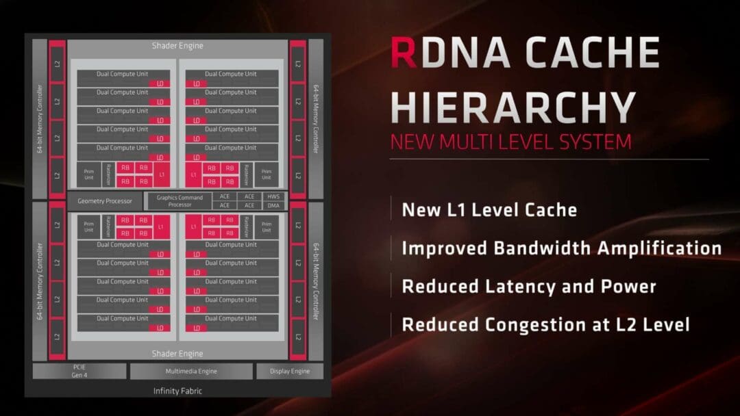
With the new RDNA based Navi design, AMD has been rather generous with the cache memory. By adding another block of L1 cache between L2 and L0, the latency has significantly improved over GCN. The L0 cache is exclusive to a Dual Compute Unit while the L1 cache is shared between four DCUs. A larger block of 4MB L2 cache is accessible globally to each CU.
NVIDIA’s Turing L2 cache size is 50% larger than Navi but there’s no intermediate in between complementing the shader cache. The L1 cache is reconfigurable between shared memory and L1 as per workloads and there is one block of 96KB L1 cache per SM. The L2 cache is common across all SMs.
The main difference between shared memory and the L1 is that the contents of shared memory can be handled by the developer, whereas the L1 cache is automatically managed. Basically, shared memory gives developers more control over the GPU resources which is a core part of DX12.
Rasterizers, Tesselators and Texture Units
Other than the Execution Units, Cache and the Graphics Engines, there are a few other components such as the Rasterizers, Texture Units and Render Backend. The rasterizer converts the 3D scene into one pixels that can be displayed on a monitor or screen, in addition to Z-culling. After the pixel shader does its thing by assigning and interpolating the color to every pixel, the ROPs perform the late Z/stencil, depth and blending tests, and order the quads as per API order and finally send it out to the display as output.

Texture sampling consists of determining the target location of the textures along the two or three coordinates and thereby calculating the texture coordinate gradients. Then using these values the MIP map levels to be sampled are (texture size to be displayed at various points on the screen) determined with the specified LOD bias. The address modes (wrap/clamp/mirror etc) are then applied to the results to get the right position in the texture to sample from (in normalized [0,1] coordinates). Finally, the normalized coordinates are converted into fixed-point pixel coordinates to sample from and using the texture array index, we can now compute the address to read texels from and perform the mapping.
Each Compute Unit in the Navi GPUs (and Turing SM for NVIDIA) contains four TMUs. There are two rasterizers per shader engine for AMD and one for every GPC (Graphics Processing Cluster) in the case of the Turing GPU block. In AMD’s Navi, there are also RBs (Render Backends) that handle pixel and color blending, among other post-processing effects. On NVIDIA’s side, that’s handled by the ROPs.
In NVIDIA’s case, the tessellation, viewport transformation, vertex fetch and output stream is performed by the various units in the PolyMorph engine.AMD, on the other hand, has doubled down on that front by adding a geometry processor for culling unnecessary tessellation and managing geometry.
Process Nodes and Conclusion
There is another architectural difference between the NVIDIA Turing and AMD Navi GPU architectures with respect to the process node. While NVIDIA’s Turing TU102 die is much bigger than Navi 10, the number of transistors per unit mm2 is higher for the latter. (https://www.easyvet.com/)
This is because AMD’s Navi architecture leverages the newer 7nm node from TSMC. NVIDIA, on the other hand, is still using the older 14nm process. Despite that though, NVIDIA GPUs are more energy-efficient than competing Radeon RX 5700 series graphics cards.
Thanks to the 7nm node, AMD has significantly reduced the gap but it’s still a testament to how efficient NVIDIA’s GPU architecture really is.
Video Encode and Decode
Both the Turing and Navi GPUs feature a specialized engine for video encoding and decoding.
In Navi 10 (RX 5600 & 5700), unlike Vega, the video engine supports VP9 decoding. H.264 streams can be decoded at 600 frames/sec for 1080p and 4K at 150 fps. It can simultaneously encode at about half the speed: 1080p at 360 fps and 4K at 90 fps. 8K decode is available at 24 fps for both HVEC and VP9.
For streamers, Turing had a big surprise. The Turing video encoder allows 4K streaming while exceeding the quality of the X264 encoder. 8K 30FPS HDR support is another sweet addition. This is an advantage over Navi only in theory though. No one streams at 8K.
Two more features that come with Turing are Virtual Link and NVLink SLI. The former combines the different cables needed to connect your GPU to a VR headset into one while the latter improves SLI performance by leveraging the high bandwidth of the NVLink interface.
VirtualLink supports up to four lanes of High Bit Rate 3 (HBR3) DisplayPort along with the SuperSpeed USB 3 link to the headset for motion tracking. In comparison, USB-C only supports four lanes of HBR3 DisplayPort or two lanes of HBR3 DisplayPort + two lanes SuperSpeed USB 3.
- Read also:
- AMD Navi vs Vega: Differences Between RDNA and GCN Architecture
- AMD vs NVIDIA