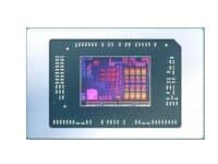
Alongside the Milan-X and Zen 4 Epyc processors, AMD today also unveiled the MI200 data center GPU (accelerator). Packing a chiplet based design, incorporating up to 14,080 stream processors across 220 CUs and two dies/chiplets, we’re looking at the most advanced accelerator ever designed. Each chiplet features eight shader engineers (total 16) with 16CUs (capable of full-rate FP64 and packed FP32 compute) each and a 2nd Gen Matrix Engine for mixed-precision compute (FP16 and BF16).
The following technologies power the Instinct MI200 lineup:
- AMD CDNA 2 architecture – 2nd Gen Matrix Cores accelerating FP64 and FP32 matrix operations, delivering up to 4X the peak theoretical FP64 performance vs. AMD previous-gen GPUs.
- Leadership Packaging Technology – Industry-first multi-die GPU design with 2.5D Elevated Fanout Bridge (EFB) technology delivers 1.8X more cores and 2.7X higher memory bandwidth vs. AMD previous-gen GPUs, offering the industry’s best aggregate peak theoretical memory bandwidth at 3.2 terabytes per second.
- 3rd Gen AMD Infinity Fabric technology – Up to 8 Infinity Fabric links connect the AMD Instinct MI200 with 3rdGen EPYC CPUs and other GPUs in the node to enable unified CPU/GPU memory coherency and maximize system throughput, allowing for an easier on-ramp for CPU codes to tap the power of accelerators.
In terms of memory and bandwidth, we’re looking at HBM2e modules. Eight channels of 1,024-bit memory controllers are connected to 16GB HBM2e stacks (8-hi), resulting in an overall capacity of 128GB (vs 80GB on the NVIDIA A100). The memory chips will run at 3.2Gbps, resulting in an overall bandwidth of 3.2TB/s, once again a good deal more than the 2TB/s possible with the A100 80GB.
The MI200 lineup consists of three SKUs, the OAM exclusive MI250 and MI250X, and the PCIe-based MI210. The MI250X consists of the fully enabled die, with 14,080 cores and an FP64 compute throughput of 383 TFLOPs. The MI215 cuts down the core count to 13,312, resulting in an FP64 throughput of 362.1 TFLOPs. The exact configuration of the MI210 remains unknown.
AMD showed off some promising numbers compared to NVIDIA’s A100 SXM. We’re looking at gains of up to 3x in HPC workloads from AMG, Quicksilver, and HPL. It’ll be interesting to see how NVIDIA’s own MCM design “Hopper” holds up against the MI200.