AMD’s Radeon RX 7000 graphics cards, otherwise known as the RDNA 3 family will be launched later this year. The top-end RX 7800 XT and 7900 XT GPUs will feature a chiplet design with the latter packing as many as 7 separate dies. Both will leverage TSMC’s 5nm and 6nm processes depending on the die and the performance tier. Meanwhile, the budget grade RX 7700 XT will be based solely on the 6nm node and for the same reason, it’ll launch much earlier than the rest.
The Navi 33 core which will power the Radeon RX 7700 XT is almost certainly in the mass production stage and awaiting the packaging and assembly process. It should launch alongside the GeForce RTX 4080/4070 in the second half of 2022. As for Navi 31 which will form the heart of the Radeon RX 7900 XT, we can expect volume production to be underway as well. The launch should be targeted for the holiday season or the first quarter of 2023.

Finally, we have the Navi 32 die which will power the Radeon RX 7800 XT. This will be the final Navi 3X part to be mass-produced. According to Greymon55, this particular SKU was taped out in the last quarter of 2021 which means mass production should begin anytime now. The RX 7800 XT should launch sometime in early 2023.
Previous Coverage on Navi 31:
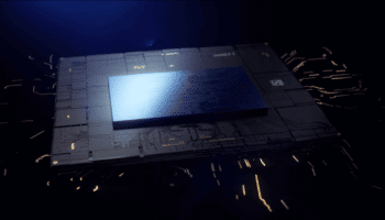
AMD’s Radeon RX 7900 XT based on the RDNA 3 graphics architecture will feature up to 7 dies (chiplets). Out of these, two will be the Graphics Compute Dies (GCDs), four Memory Controller Dies (MCDs), and the Active Bridge Interconnect (ABI).
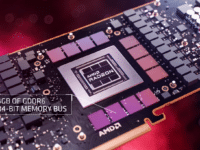
The GCDs pack the main processing cluster across two identical dies. Each die will consist of 7,680 stream processors (cores) across 6 shader arrays and 3 shader engines. This results in an overall shader count of 15,360 spread across 12 shader arrays and 6 shader engines. The overall bus width is expected to be 256-bit with the memory controllers divided equally across the two dies.
With the 2nd Gen RDNA 2 GPUs, the L3 cache was on the GPU core die. However, with the Radeon RX 7900 XT/7800 XT, it has reportedly been shifted to separate cache/memory controller dies. There will be four cache/memory controller dies. These will pack a total last level cache of up to 256MB (512MB scrapped?).
Finally, there’s the Active Bridge Interconnect (ABI) which will pair the compute dies. This is reportedly going to be 3D stacked atop the GCDs. Initially, it was thought that the ABI would contain the L3 cache above the GCDs but I’m not sure if that’s the case anymore. It’s important to remember that the last part is based on speculation. That one lone die could be the I/O die or something else entirely, so take it with a grain of salt.