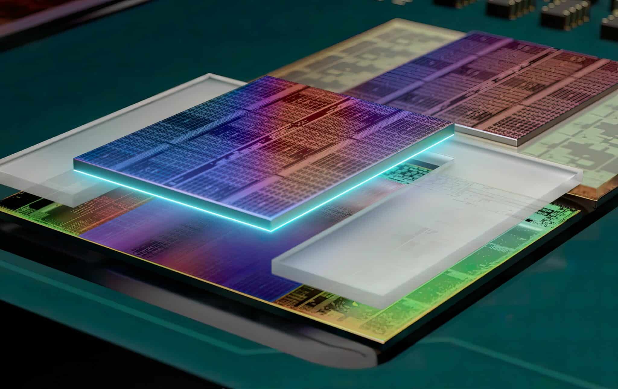
TSMC’s 3nm process node is the most expensive manufacturing technology in the semiconductor industry’s history. With a steep price of $20,000 per wafer, it offers a logic density and efficiency gain of 60% and 30-35%, respectively. Rumors claimed that the yield rates of the 3nm process are abysmal (<50%), but TSMC has clarified that overall defect rates are in-line or higher than the initial tape-outs of the 5nm process.
Without a doubt, pricing is the primary factor limiting industry adoption. For the time being, Apple is the only client set to leverage the cutting-edge process node. TSMC’s second and third largest customers, AMD and MediaTek, have yet to detail any products based on the N3 node.
AMD’s next-gen Zen 5 core architecture is expected to leverage either the N4 or the N3 process, depending on yields and pricing. In the latter case, a Q4 2024 launch is the best-case scenario. To maximize margins, NVIDIA will use the N4 or a cheaper Samsung node for its RTX 50 series GPUs. As for Qualcomm and MediaTek, custom 5nm nodes may be the best way forward.
To attract longstanding and new clients, TSMC plans to reduce 3nm (N3) wafer pricing in the coming years. The main benefactors of this reduction will be AMD, NVIDIA, MediaTek, and Qualcomm. These IC design companies account for most of TSMC’s wafer revenue.
Source: Mydrivers
-
 AMD Zen 5 Strix Point/Halo, Granite Ridge & Turin: Ryzen 9000 Specs, News & Rumors
-
 NVIDIA RTX 5080 Mobile Allegedly Based on GB203 GPU, GDDR7 Memory & PCIe Gen 5
-
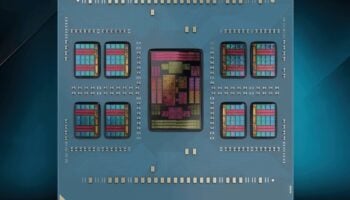 AMD’s Zen 5 Being Sampled: Ryzen 9000 CPUs incl. Mobile Chips Launch Later This Year
-
 AMD Radeon RX 7900 XT Drops Below $700 (-$210 Off), RX 6800 at $369 (-$310 Off)