The folks over at the 3D Center have been looking at the possible designs of AMD’s next-gen Navi 3X (RDNA 3) lineup of GPUs which are going to be the first consumer product stack to leverage a chiplet design. We already know that Navi 33 is going to be the successor to Navi 21 with the same CU count of 80 and 128MB of L3 cache. The most interesting SKU is Navi 31 which will supposedly feature two Navi 33 dies to increase performance by at least 50% over the single monolithic design.
The latest patents indicate that there won’t be a separate I/O die and the memory controllers will be local to the master die with each slave chiplet having its own set of memory channels attached to the L3 cache on the active bridge chiplet. This means that if a single GPU chiplet has a bus width of 64-bits, two will result in a GPU with a bus width of 128-bit and three in 192-bit. Looking at the above designs, the third one seems closest to this, with two compute dies connected by the active L3 cache bridge to help synchronize them. The existence of a separate MCD is unlikely as we haven’t seen any evidence of one in either the MI200 or Navi 3x leaks.

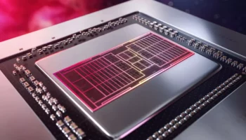
The above picture from the recently leaked patent is a good illustration of AMD’s approach to chiplet GPUs. However, we won’t be seeing three compute dies with the first iteration and a dual-die design is the most likely candidate. Read more: