The specifications of NVIDIA’s AD102 “Lovelace” GPU die have been finally confirmed. The fully enabled core will pack an incredible 18,432 FP32 cores, a sizable increase over the AMD Navi 31’s 12,288 shaders. As reported the other day, the RTX 4090 will come with a couple of GPCs partially fused off, bringing down the effective core count to 16,128. If NVIDIA ever plans to launch a 4090 Ti that behemoth will leverage the full-fat AD102 core and its 18,432 shaders.
Forget it. Still up to 18432. 🤪🤪🤪🤪🤪 Confirmed.

— kopite7kimi (@kopite7kimi) May 18, 2022

According to Kopite7kimi, the AD102 die will be able to touch the 100 TFLOPs single-precision performance mark with its core running at 2.8GHz. What he still isn’t sure about is the SM structure. NVIDIA has a habit of mildly restructuring its SM (Compute Unit) every generation. This time around it might be thoroughly overhauled, much like with Maxwell roughly eight years back, or not.
I’ll recap what I had shared a while back about the Maxwell SM and the possible SM design of Lovelace:
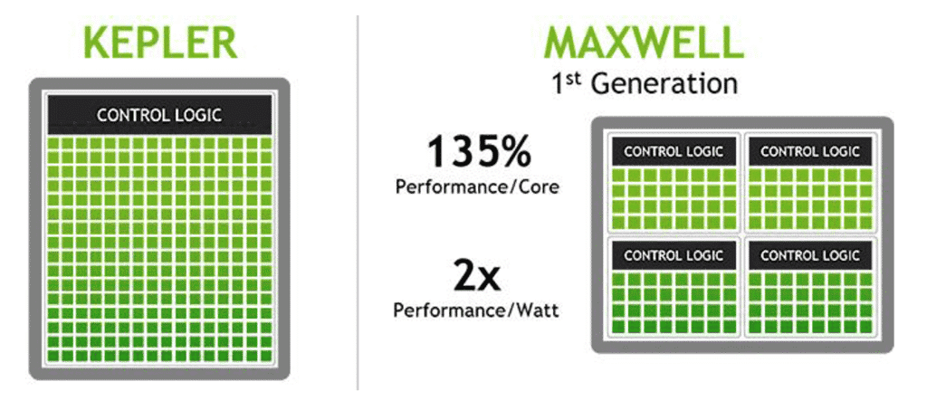
With Maxwell, the warp schedulers and the resulting threads per SM/clock were quadrupled, resulting in a 135% performance gain per core. It looks like NVIDIA wants to pull another Maxwell, a generation known for exceptional performance and power efficiency that absolutely crushed rival AMD’s Radeon offerings.
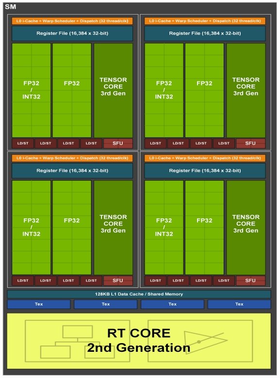
This would mean that the overall core count per SM would remain unchanged (128) but the resources accessible to each cluster would increase drastically. Most notably, the number of concurrent threads would double from 128 to 256. It’s hard to say how much of a performance increase this will translate to but we’ll certainly see a fat gain. (classicsofttrim.com) Unfortunately, this layout takes up a lot of expensive die space, something NVIDIA is already paying a lot of dough to acquire (TSMC N4). So, it’s hard to say whether Jensen’s team actually managed to pull this off or shelved it for future designs.
There’s also a chance that Team Green decides to go with a coupled SM design, something already introduced with Hopper. In case you missed out on the Hopper Whitepaper, here’s a small primer on Thread Block Clusters and Distributed Shared Memory (DSM). To make scheduling on GPUs with over 100 SMs more efficient, Hopper and Lovelace will group every two thread blocks in a GPC into a cluster. The primary aim of Thread Block Clusters is to improve multithreading and SM utilization. These Clusters run concurrently across SMs in a GPC.
Thanks to an SM-to-SM network between the two threads blocks in a cluster, data can be efficiently shared between them. This is going to be one of the key features promoting scalability on Hopper and Lovelace which is a key requirement when you’re increasing the core/ALU count by over 50%.
| GPU | GA102 | AD102 | RTX 4090 | AD103 | RTX 4080 | RTX 4070 Ti (AD104) | RTX 4070 |
|---|---|---|---|---|---|---|---|
| Arch | Ampere | Ada Lovelace | Ada Lovelace | Ada Lovelace | |||
| Process | Sam 8nm LPP | TSMC 5nm | TSMC 5nm | TSMC 5nm | |||
| GPC | 7 | 12 | 11 | 7 | 7 | 5 | 5 |
| TPC | 42 | 72 | 64 | 42 | 40 | 30 | 30 |
| SMs | 84 | 144 | 128 | 84 | 80 | 60 | 60 |
| Shaders | 10,752 | 18,432 | 16,384 | 10,752 | 9,728 | 7,680 | 7,680 |
| TP | 37.6 | ~100 TFLOPs? | 83 TFLOPs | ~50 TFLOPs | 47 TFLOPs? | ~35 TFLOPs | 35 TFLOPs? |
| Memory | 24GB GDDR6X | 48GB GDDR6X | 24GB GDDR6X | 16GB GDDR6X | 12GB GDDR6X | ||
| L2 Cache | 6MB | 96MB | 72MB | 64MB | 48MB | ||
| Bus Width | 384-bit | 384-bit | 256-bit | 192-bit | |||
| TGP | 350W | 600W | 450W | 450W | 285-340W | 300W | 285W |
| Launch | Sep 2020 | Sept 22? | Sept 22? | Q1 2023? |
These are the two potential ways NVIDIA can (nearly) double the core counts without crippling scaling or leaving some of the shaders underutilized. Of course, there’s always a chance that Jensen’s team comes up with something entirely new and unexpected.