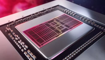
NVIDIA plans to launch its next-gen Hopper data center GPUs later this year, with a possible announcement at GTC 2022 in late March. Based on a chiplet design, the GH100 will accelerate inferencing and other machine learning workloads, while also pushing record big data and HPC performance. The GH100 full-fat die will pack a total of 144 SMs (Streaming Multiprocessors) across 8 GPCs (Graphics Processing Clusters), and 72 TPCs (Texture Processing Clusters).
| Data Center GPU | NVIDIA Tesla P100 | NVIDIA Tesla V100 | NVIDIA A100 | NVIDIA H100 |
|---|---|---|---|---|
| GPU Codename | GP100 | GV100 | GA100 | GH100 |
| GPU Architecture | NVIDIA Pascal | NVIDIA Volta | NVIDIA Ampere | NVIDIA Hopper |
| SMs | 56 | 80 | 108 | 144 |
| TPCs | 28 | 40 | 54 | 72 |
| FP32 Cores / SM | 64 | 64 | 64 | 64 |
| FP32 Cores / GPU | 3584 | 5120 | 6912 | 9216 |
| FP64 Cores / SM | 32 | 32 | 32 | 32 |
| FP64 Cores / GPU | 1792 | 2560 | 3456 | 4608 |
| INT32 Cores / SM | NA | 64 | 64 | 64 |
| INT32 Cores / GPU | NA | 5120 | 6912 | 9216 |
| Tensor Cores / SM | NA | 8 | 42 | ? |
| Tensor Cores / GPU | NA | 640 | 432 | ? |
| Texture Units | 224 | 320 | 432 | 576 |
| Memory Interface | 4096-bit HBM2 | 4096-bit HBM2 | 5120-bit HBM2 | 6144-bit HBM3? |
| Memory Size | 16 GB | 32 GB / 16 GB | 40 GB | 128GB? |
| Memory Data Rate | 703 MHz DDR | 877.5 MHz DDR | 1215 MHz DDR | 1600 MHz DDR? |
| Memory Bandwidth | 720 GB/sec | 900 GB/sec | 1555 GB/sec | ? |
| L2 Cache Size | 4096 KB | 6144 KB | 40960 KB | 96000 KB? |
| TDP | 300 Watts | 300 Watts | 400 Watts | 500W? |
| TSMC Manufacturing Process | 16 nm FinFET+ | 12 nm FFN | 7 nm N7 | 5 nm N5 |
The key upgrade over Ampere is the one additional TPC per SM, bringing up the total to 72 (each GPC packing 9 TPCs). This increases the overall ALU count by 30-35%, bringing the FP32 figure to 9,216, and FP64 to 4,608. If Hopper will actually leverage a chiplet approach, then we’re probably looking at just one of the two dies making up the entire SKU.
Running the numbers, you get a total of 288 SMs, 144 TPCs, 16 GPCs, resulting in an overall core count of 18,432 and 9,216 for the FP32 and FP64 ALUs, respectively. If NVIDIA wants to overcome AMD’s recently announced Instinct MI200 family, then these figures are kind of necessary.
The memory pool will also grow quite significantly with Hopper, increasing from “just” 40GB HBM2 on the GA100 to at least 128GB of HBM3 on the GH100. HBM 3 allows for 24GB stacks across a 1,024-bit bus which means NVIDIA can use up to 16-24GB stacks acoss six 1,204-bit memory controllers. The L2 cache is another mystery, but considering that the GA100 already had over 40MB, it’s probable that we’ll see 96MB on the GH100, the same as the AD102.