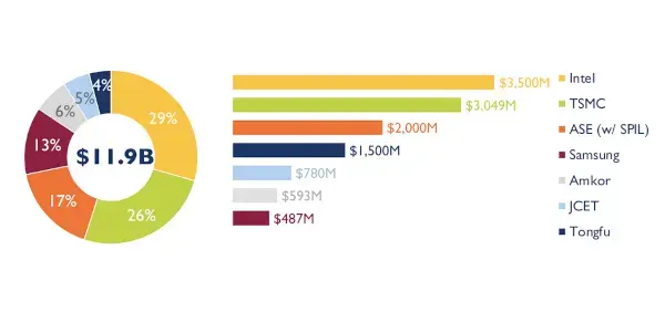
Intel is the strongest believer in advanced 2.5D and 3D stacking technologies, going by its investments in the segment last year. The chipmaker spent a considerable $3.5 billion USD on the high-end performance packaging market in 2021. The bulk of it went into the advancement of Foveros and EMIB. The former is a 2.5D packaging technique used to connect dies on the same substrate. Its 2.5D packaging uses an embedded multi-die interconnect bridge (EMIB) based on a 55-micron bump pitch.
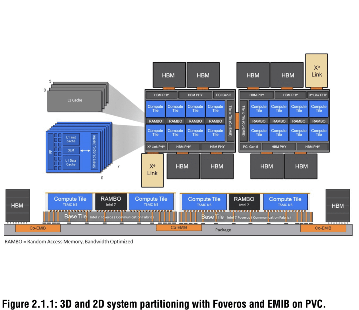
Foveros, on the other hand, is a 3D stacking tech, initially used in Lakefield to stack DRAM upon compute dies. In the near future, it will be leveraged in Ponte Vecchio, to stack the compute and cache tiles atop the Intel 7 Foveros tiles. Combined with EMIB, this implementation is called Co-EMIB.
Following closely behind Intel, we have TSMC which spent $3.05 billion USD on packaging technologies in 2021. Unlike Intel, TSMC’s advanced packaging techniques are used by a wide range of chipmakers, including AMD, Apple, Qualcomm, and MediaTek. AMD’s Ryzen 7 5800X3D, and the Milan-X server processors, for example, use the CoWoS platform for 3D stacking L3 cache dies atop the base compute die.

Samsung Foundry lags behind its rivals by quite a bit here. It spent less than $500 million on advanced packaging development in 2021. Its X-Cube technology is used by chipmakers to 3D stack memory dies, most notably HBM. X-Cube (eXtended-Cube) uses a 7nm TSV process and is set to use hybrid bonding interconnects.