With Alder Lake, Intel is, for the first time, moving to a hybrid core architecture across its entire product stack from the 9-15W U15 to the 125W desktop “S” lineup. Alder Lake will combine two different core architectures, namely Golden Cove and Gracemont (both 10nm ESF) for a more flexible approach to performance and power efficiency. While this may look like a simple fix to make the processors more power-efficient, the reality is more complicated. The OS scheduler should be able to smartly distinguish between the two and decide which workloads are best suited for each core cluster. Furthermore, the ISAs supported by the two architecture aren’t identical. The “small” Atom cores don’t support all the instructions supported by the “big” core, the most notable being AVX2 and FMA with Tremont. As such, when an application leveraging these kinds of instructions is run on Tremont, they’ll be quite a bit slower than on Skylake.
In this post, I’d like to take a look at the predecessor of the upcoming Gracemont core (which will be the low-power core in Alder Lake) and compare it to Skylake which has basically become “de-facto” architecture (not quite literally, mind you) over the last 4-5 years. As such, if GC is able to offer performance comparable to Skylake or outperform it, then it’ll be hard to look at it as just a low-power alternative. Instead, these cores should perform similar to the older -Lake processors in most workloads even when the Golden Cove cores are idle. We’ll have a look at the ISAs, the front end, back end, and frequencies of the two core architectures and see how the Atom architecture has matured over the years.
Intel Big Core vs Small Core: Tremont vs Skylake, Frontend & Backend
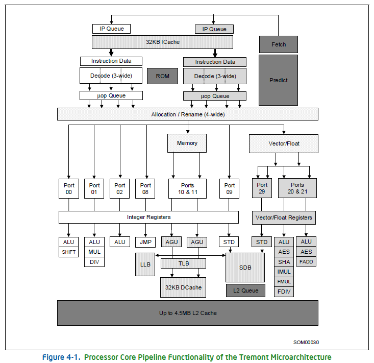
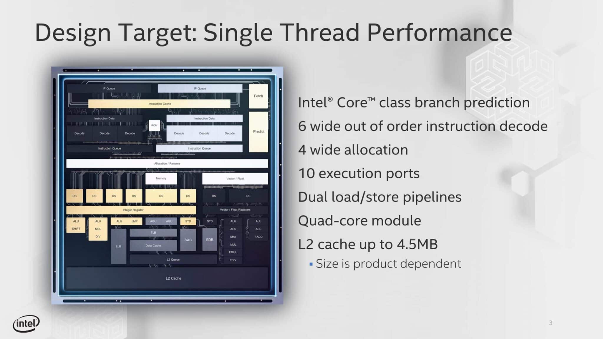
Bear in mind that while comparing Gracemont (a yet unreleased architecture) to a 5-year-old design isn’t entirely fair, it’s worth noting that at the moment, 75% or more of the total Blue userbase is still using some form of Skylake. Since we still don’t have the block diagram for Gracemont, we’ll be using Tremont for reference with some speculation here and there. Starting with the branch predictor, Tremont has a Core-class predictor that performs very similarly to Skylake with some compromises to the prediction table size. Gracemont should be even closer if not better than Skylake in terms of the BP. The fact that the latter uses a 14nm node while the former is based on the newer 10nm process should have afforded the required die area.
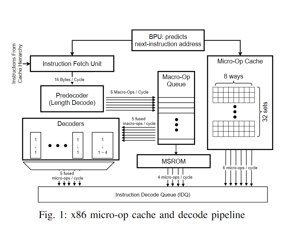
Tremont has a very interesting instruction decoder. It features two 3-wide decoders, each of which is fed by a separate stream of (16Bx2) instructions from the L1I cache. Unlike Skylake (and Sunny Cove), Tremont doesn’t have a separate pre-decode stage (or macro-fusion?). While this shouldn’t really matter much, the lack of an op-cache should make a notable difference. Skylake has four 1:1 decoders and one 1:4 complex decoder in addition to a micro-op cache capable of supplying up to 6 micro-ops per cycle. Tremont essentially has just a three-wide decoder.
The primary advantage of a dual-decoder is that the two are separately fed and as such when dealing with two different branch predictions can take undertake them both simultaneously. However, when there’s no branch (rare, but it happens), one of the decoders is turned off to save power. While Intel’s whitepaper states otherwise, the lack of a micro-op-cache should have a notable impact on the capabilities of the front-end. Overall, Tremont (and therefore, Gracemont) have a well-built frontend, capable of keeping the backend well-fed in most scenarios.
[It’s possible that we will see one with Gracemont as Sunny Cove boosted its capacity by 50% compared to Skylake. Even with older architectures such as Ivy and Sandybridge, the op-cache boosts throughput by 20-25%. This has only increased over generations and is highly unlikely that Tremont or Gracemont would perform worse without one. AMD uses a standard x86 decoder capable of decoding four macro-instructions per cycle, with the micro-op cache delivering up to eight cached instructions, making it much more effective than the standard decode pipeline. It’s for this reason that u-op caches of most modern processors have a high hit rate of over 75% in most cases..]
Another advantage that Skylake has is that it can fuse multiple similar micro-ops into one single instruction which can then be processed in one go. Tremont seems to lack this, and it’s unlikely that we’ll see it patched into Gracemont.
The most noteworthy parts of the backend include the ReOrder Buffers, the Execution Units, and the register files. Tremont has a fairly large ROB capable of holding 208 instructions, versus 224 on Skylake and 352 on Sunny Cove. The major difference between Intel’s big and small cores here is with respect to the reservation station (instruction scheduler) where micro-ops wait for execution or use for register renaming. While Skylake and Sunny Cove have a single (large) RS containing up to 97 entries, Tremont (and most likely GM) have individual stations for each port. The two vector EUs have a shared reservation and so do another pair of Address Generation Units (AGUs) for two 16-byte stores/loads, or one of each.
Skylake can do two loads and one store per cycle while four ports being dedicated to them. Furthermore, while Tremont has separate ports for integer and floating-point execution, Skylake and Sunny Cove share common ports for both. The other difference is with respect to the ALUs themselves. While Skylake has multiple 256-bit vector units, Tremont is limited to 128b wide EUs, although Gracemont is almost certainly expected to the 256b units to support native AVX2 and FMA.
L1 and L2 Cache: Tremont/Gracemont vs Skylake
Tremont has a 1024-entry L2 TLB while Sunny Cove can contain up to 2,048. In comparison, Skylake could hold up to 1,536 entries and Zen 3 is limited to just 512. Similar to Sunny Cove, both Zen 2 and Zen 3 have an 8-way 32KB L1I cache, with the L1 Branch Target Buffer being doubled to 1,024 entries (512 on Zen 2) on Zen 3, L0 being unchanged at 16, and L2 BTB slightly wider at 6.5K (6K on Zen 2).
| Gracemont | Tremont | Goldmont+ | Goldmont | Sunny Cove | Skylake | |
|---|---|---|---|---|---|---|
| Process | 10nm ESF | 10nm+ | 14nm++ | 14nm | 10nm+ | 14nm++ |
| Decode | 4-6 way? | 2×3-way | 3-way | 3-way | 5-way | 5-way |
| Allocate | 4-wide? | 4-wide | 4-wide | 3-wide | 10-wide | 8-wide |
| L1 Instruction | 64 KB 16-way | 32 KB 8-way | 32 KB 8-way | 32 KB 8-way | 32 KB 8-way | 32 KB 8-way |
| L1 Data | 32 KB 8-way | 32 KB 8-way | 24 KB 6-way | 24 KB 6-way | 48 KB 12-way | 32 KB 8-way |
| L1 Latency | 3-cycle | 3-cycle | 3-cycle | 3-cycle | 5-cycle | 4-cycle |
| L2 Cache | 1.5MB | 1.5 12-18 way | 1.0 MB 16-way | 0.5-1.0 MB 16-way | 512 KB 8-way | 256 KB 4-way |
| L2 Latency | 17-cycle? | 17-cycle | 19-cycle | 17-cycle | 13-cycle | 12 cycle |
Tremont has an L1D cache size of 32KB with 8-way associativity, and so is the L1I cache. Gracemont is expected to expand the latter to 64KB/core with 16-way associativity. Skylake also has the same L1 cache size as Tremont, although with a higher latency of 4-cycles. Sunny Cove has a larger 48KB 12-way L1D cache but an even higher latency of 5-cycles. Tremont and Gracemont should both have a relatively lower 3-cycle latency.
Tremont has an L2 cache of up to 4MB for a set of four cores (a module), with each core having access to roughly 1.5MB of it. This is a fair bit more than Skylake and even Sunny Cove, but a larger capacity means higher latency as well.
Instructions and Frequencies: Tremont/Gracemont vs Skylake
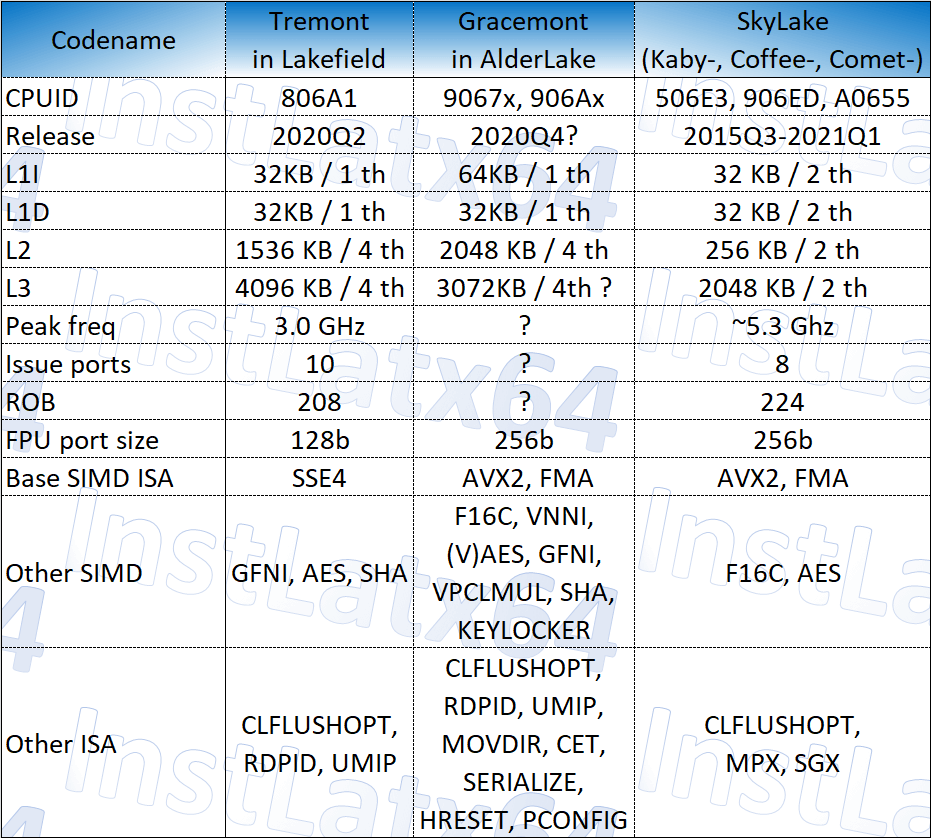
Finally, there’s the matter of the supported instructions across the two different architectures. While Tremont lacks support for AVX2 or FMA on a native level, Gracemont is expected to support both, putting it more or less on par with Skylake in terms of commonly used ISAs. There are still a few instructions that will be missing on the Monts such as AVX512, SGX, and AMX, but that should be of little to consequence to the average user.
At the end of the day, what will eventually hold back the Gracemont cores compared to Skylake are the operating frequencies. While newer Skylake designs remained relevant by hitting boost clocks of 5GHz+, and all-core frequencies close to 5GHz, the former is expected to stay below the 3.5GHz mark. This means that despite near architectural parity, there should be a notable delta between the two. The fact that Tremont has a base clock of 1.5-2GHz should further reiterate that. However, these are low power cores, and to stay “low-power” have been designed to operate in this frequency range. To answer the original question, yes, Gracemont should be nearly as capable as Skylake, but it can be thought of as a low-power Skylake core running in power-saving mode, with there being a notable performance delta between the two.
Related reading:
