Nearly all kinds of volatile memory is based on dynamic random access memory or DRAM.
DDR4 runs between 1200 to 1600MHz. OEMs often advertise DDR4 speeds as DDR4-3200 or DDR4-3600. This isn’t the operating frequency but the number of MT/s (million transfers per sec). In DDR4 memory, two transfers occur per cycle (Double Data Rate) which is why the effective data rate is twice the frequency: 3600MT/s for 1800MHz and 3200MT/s for 1600MHz.
DDR4 is the latest iteration of DRAM. Released in 2014, it initially focused on reducing the voltage and power consumption rather than increasing the operating frequencies. With the coming of AMD’s Ryzen processors and the MCM design
DDR4 vs DDR3
Aside from the obvious (faster frequencies and lower latency), the primary advantages of DDR4 memory over DDR3 are higher DIMM sizes (up to 64 GB, DDR3 is limited to 16GB) and a considerably lower operating voltage. While running at 1200 to 1600MHz, DDR4 operates at a voltage of 1.2v, while DDR3 had a voltage of 1.5v, all the while running between 400 and 1067MHz.
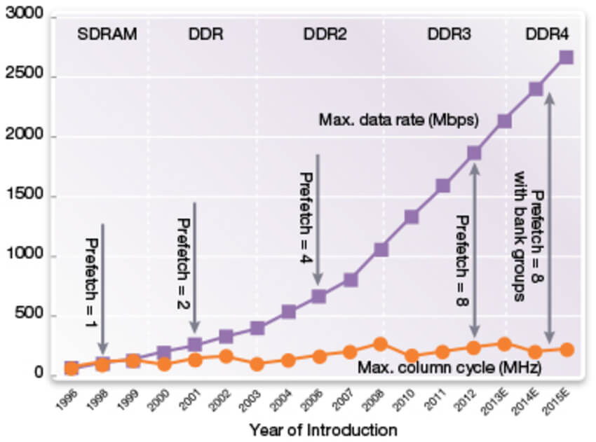
Unlike the transition from DDR2 to DDR3, the move to DDR4 didn’t increase the burst length or prefetch. Both DDR3, as well as DDR4, has a burst length of 8 and an 8n prefetch.
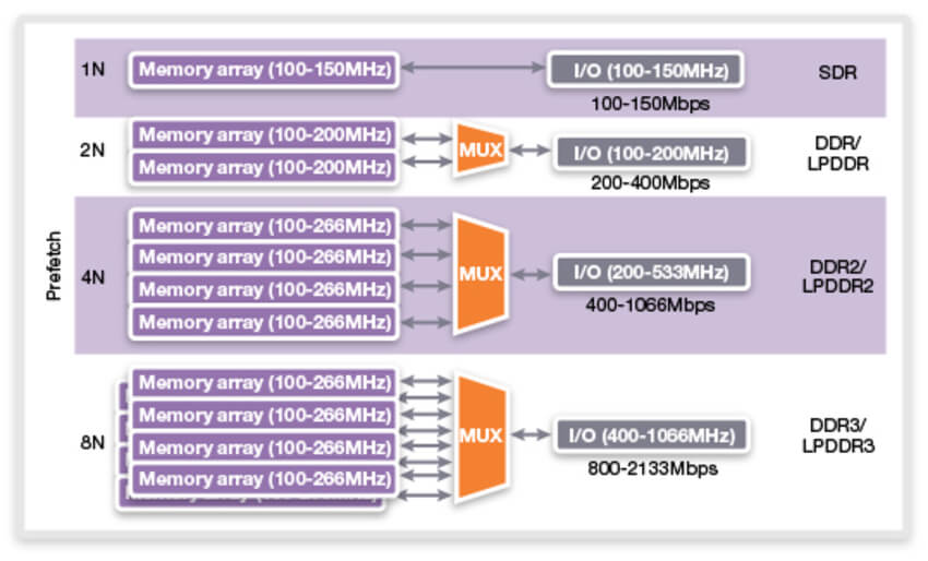
However, there is one key difference in the memory bank groups of DDR3 and DDR4 memory. As you can see above, DDR3 has an 8n prefetch with four memory arrays forming a bank group connected via a multiplexer to the I/O controller.
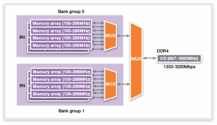
Although DDR4 maintains the same 8n prefetch and burst length as DDR3, it has two memory bank groups per channel. The two bank groups are separate and can execute two independent 8n prefetches. This is done by using a multiplexer to time division multiplex its internal banks. Therefore, the effective prefetch for DDR4 is wider than DDR3.
DDR4 vs DDR5 Memory
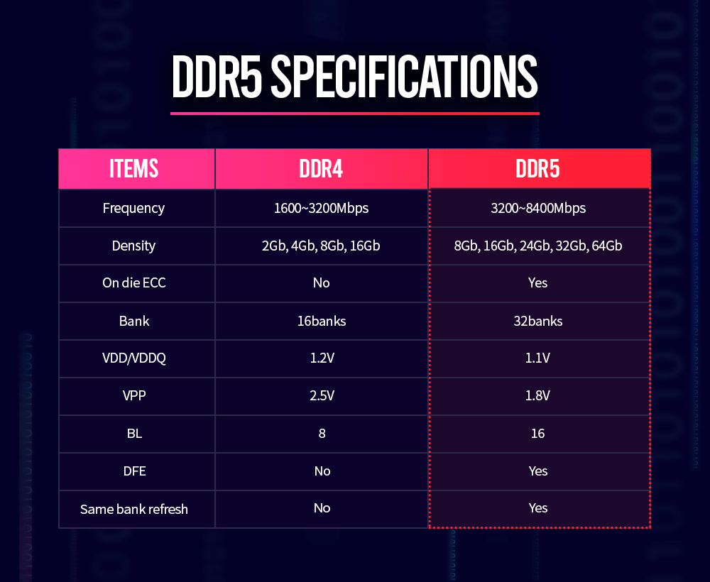
The specifications of the next-gen DDR5 memory standard have been announced and they’re a substantial step above the existing DDR4 modules. DDR5 aims to reach bandwidths as high as 4800Mbps per DIMM, a hefty 50% gain over DDR4’s 3200Mbps. This massive uplift is achieved via the following advances in the memory structure:
32-Bank Structure: DDR5 uses a 32 bank structure with 8 bank groups, twice as much as DDR4’s 16 bank design. This effectively doubles the memory access availability. To complement this, DDR5 also adopts the Same Bank Refresh Function. Unlike DDR4, this allows the next-gen memory to access other memory banks while the rest are operating or refreshing.
Burst Length: With DDR4, the burst rate was limited to 8, allowing transfers of up to 16B from the cache at a time. DDR5 increases this to 16, with support for 32-length mode, which allows up to 64-byte cache line fetch with just one DIMM.
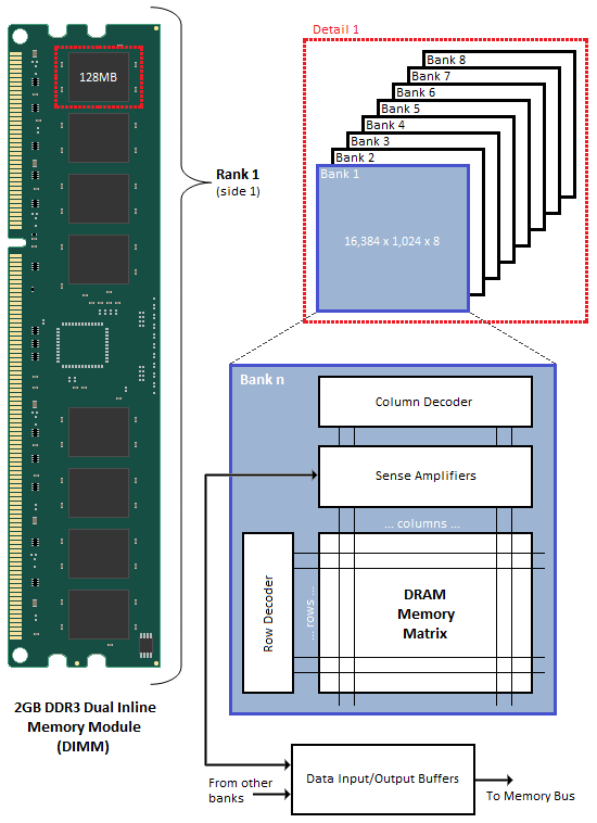
To understand what burst-length means, you need to know how memory is accessed. When the CPU or cache requests new data, the address is sent to the memory module and the required row, after which the column is located (if not present, a new row is loaded). Keep in mind that there’s a delay after every step.
Then the entire column is sent across the memory bus, but instead in bursts. For DDR4, each burst was 8 (or 16B). With DDR5, it has been increased to 16 with further scope up to 32 (64B). There are two bursts per clock and they happen at the effective data rate.
16n Prefetch: The prefetch has also been scaled up to 16n to keep up with the increased burst length. Like DDR4, there will be two memory-bank arrays per channel connected via a MUX resulting in a higher effective prefetch rate.
- By adopting a Decision Feedback Equalization (DFE) circuit, which eliminates reflective noise during the channels’ high-speed operation, DDR5 increases the speed per pin considerably.
| Feature/Option | DDR4 | DDR5 | DDR5 Advantage |
|---|---|---|---|
| Data rates | 1600-3200 MT/s | 3200-6400 MT/s | Increases performance and bandwidth |
| VDD/VDDQ/VPP | 1.2/1.2/2.5 | 1.1/1.1/1.8 | Lowers power |
| Internal VREF | VREFDQ | VREFDQ, VREFCA, VREFCS | Improves voltage margins, reduces BOM costs |
| Device densities | 2Gb-16Gb | 8Gb-64Gb | Enables larger monolithic devices |
| Prefetch | 8n | 16n | Keeps the internal core clock low |
| DQ receiver equalization | CTLE | DFE | Improves opening of the received DQ data eyes inside the DRAM |
| Duty cycle adjustment (DCA) | None | DQS and DQ | Improves signaling on the transmitted DQ/DQS pins |
| Internal DQS delay monitoring | None | DQS interval oscillator | Increases robustness against environmental changes |
| On-die ECC | None | 128b+8b SEC, error check and scrub | Strengthens on-chip RAS |
| CRC | Write | Read/Write | Strengthens system RAS by protecting read data |
| Bank groups (BG)/banks | 4 BG x 4 banks (x4/x8) 2 BG x 4 banks (x16) | 8 BG x 2 banks (8Gb x4/x8) 4 BG x 2 banks (8Gb x16) 8 BG x 4 banks (16-64Gb x4/x8) 4 BG x 4 banks (16-64Gb x16) | Improves bandwidth/performance |
| Command/address interface | ODT, CKE, ACT, RAS, CAS, WE, A<X:0> | CA<13:0> | Dramatically reduces the CA pin count |
| ODT | DQ, DQS, DM/DBI | DQ, DQS, DM, CA bus | Improves signal integrity, reduces BOM costs |
| Burst length | BL8 (and BL4) | BL16, BL32 (and BC8 OTF, BL32 OTF) | Allows 64B cache line fetch with only 1 DIMM subchannel. |
| MIR (“mirror” pin) | None | Yes | Improves DIMM signaling |
| Bus inversion | Data bus inversion (DBI) | Command/address inversion (CAI) | Reduces VDDQ noise on modules |
| CA training, CS training | None | CA training, CS training | Improves timing margin on CA and CS pins |
| Write leveling training modes | Yes | Improved | Compensates for unmatched DQ-DQS path |
| Read training patterns | Possible with the MPR | Dedicated MRs for serial (userdefined), clock and LFSR-generated training patterns | Makes read timing margin more robust |
| Mode registers | 7 x 17 bits | Up to 256 x 8 bits (LPDDR type read/write) | Provides room to expand |
| PRECHARGE commands | All bank and per bank | All bank, per bank, and same bank | PREsb enables precharging-specific bank in each BG |
| REFRESH commands | All bank | All bank and same bank | REFsb enables refreshing of specific bank in each BG |
| Loopback mode | None | Yes | Enables testing of the DQ and DQS signaling |
- DDR5 also increases the memory density all the way (up) to 64Gb from 16Gb and both the VDD and VPP voltages have gone down from 1.2v to 1.1v to reduce the power draw.
- At the same time, DDR5 will also bring operating clocks as high as 4200MHz (or 8400MT/s) while DDR4 was limited to 1600MHz (or 3200MT/s).
- Lastly, similar to LPDDR4 and 5, DDR5 will limit the bus width to 32-bit (40-bit for ECC) per channel, but at the same time use two channels per DIMM. In turn, some OEMs will be using quad-channel memory instead of dual-channel to make up for this.
Finally, on-chip ECC has also been added and the Mode Registers have also been significantly upgraded. You can see the entire change-list in the above table.
