Intel and AMD have been the defacto processor manufacturing/design firms for more than 50 years now. Although both use the x86 ISA to power their chips, their approach to CPU design has taken completely different paths over the last decade or so. Things started to change after AMD spun off Global Foundries as a separate unit and started relying on TSMC for its supply of chips.
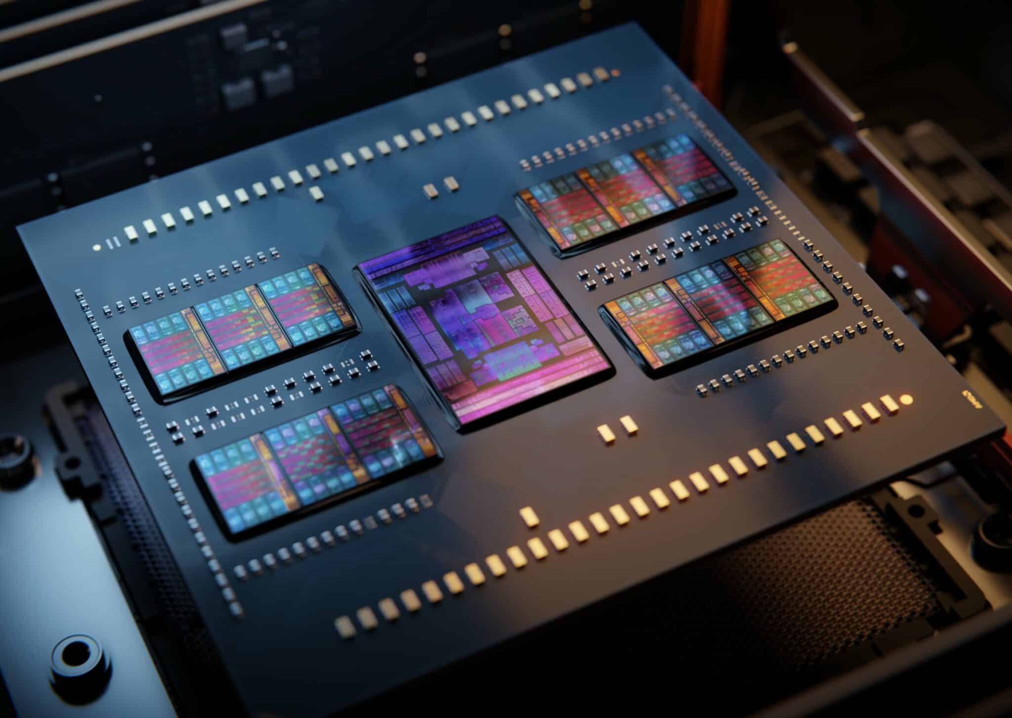
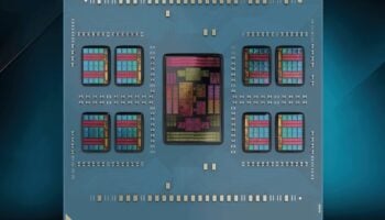
The Bulldozer debacle left Team Red in a precarious situation. It needed a low-cost solution to compete with Intel’s much more advanced architectures. The result was Zen. Leveraging a chiplet or MCM (multi-chip module) architecture, the Ryzen processors marked a radical shift in the PC and chipmaking industry as a whole.
The 1st Gen Ryzen architecture was relatively simple: An SoC design with everything from cores to I/O and controllers on the same die. The CCX concept was introduced, wherein CPU cores were grouped into four-core units and combined using the Infinity Cache. Two quad-core CCXs formed a die.
It’s important to note that even though the CCXs were introduced, the consumer Ryzen chips were still monolithic single-die designs. Furthermore, although the L3 cache was shared across all the cores in a CCX, each had its own slice. Accessing the last level cache (LLC) of another was relatively slower, even more so if it was on the other CCX. This caused poor performance in latency-sensitive applications like gaming.
Things largely remained the same with Zen+ (-node shrink), but Zen 2 was a major upgrade. It was the first chiplet-based design for consumer CPUs featuring two compute dies or CCDs and one I/O die. AMD added a second CCD on the Ryzen 9 parts for core counts never seen before on the consumer front.
The 16MB L3 cache was more accessible (read: faster) for all the cores on the CCX, greatly improving gaming performance. The I/O die was separated, and the Infinity Fabric was upgraded. At this point, AMD was slightly slower in gaming but offered superior content creation performance than rival Intel Core chips.
Zen 3 further refined the chiplet design, eliminating the CCX and merging the eight cores and 32MB cache into one unified CCD. This drastically reduced cache latency and simplified the memory sub-system. For the first time, AMD’s Ryzen processors offered better gaming performance than archrival Intel’s. Zen 4 makes no notable changes to the CCD design other than making them smaller.
Intel: Monolithic for Now, Tiles Coming Soon
Continued on the next page…
Intel has been following a monolithic approach to processor design. Essentially, this means that all cores, cache, and I/O resources for a given processor are physically on the same monolithic chip. There are some clear advantages to this approach.
The most notable is reduced latency. Since everything is on the same physical substrate, different cores take much less time to communicate, access the cache, and access system memory. Latency is reduced. This leads to optimal performance.
If everything else is the same, the monolithic approach will always net you the best performance. There’s a big drawback, though. This is in terms of cost and scaling. We need to take a quick look now at the economics of silicon yields. Strap in: things are going to get a little complicated.
Defects and Yields
When foundries manufacture CPUs (or any piece of silicon), they rarely manage 100 percent yields. Yields refer to the proportion of usable parts made. If you’re on a mature process node like TSMC’s N7 (7nm), your silicon yields will be more than 80%. You get a lot of usable CPUs with minimal wastage. The inverse is that for every 10 CPUs you manufacture, you have to discard at least 2-3 defective units. The discarded unit costs money to make, so that cost has to factor into the final selling price.
At low core counts, a monolithic approach works fine. This largely explains why Intel’s mainstream consumer CPU line has, until Ryzen, topped out at 4 cores. Increasing the core count on a monolithic chip dramatically increases costs.
On a high-end monolithic die, every (or nearly every) core has to be functional. If you’re fabbing an eight-core chip and 7 out of 8 cores work, you still can’t use it. Remember what we said about yields being more than 80 percent?
Mathematically, that ten percent defect rate stacks for every additional core on a monolithic die to the point that with, say, a 28-core Xeon, Intel has to throw away one or two defective chips for every usable one since all 28 cores have to be functional. Costs don’t just scale linearly with core count–they scale exponentially because of wastage.
The economics are much more forgivable with the chiplet approach, as costs scale linearly with core counts. Because AMD’s wastage rate is relative to its ability to create a functional 4-core block at most (a single CCX), they don’t have to throw out massive stocks of defective CPUs.
The second advantage comes from their ability to leverage those defective CPUs themselves. Whereas Intel mostly throws them out, AMD disables functional cores on a per-CCX basis to achieve different core counts.
Chiplet or Monolithic: Which is Better?
The chiplet approach is going to see widespread adoption in the coming years, from both AMD as well as Intel, for CPUs as well as GPUs. Moore’s law–which mandated a doubling in processing power, mainly due to die shrinks (56nm to 28nm> 28nm to 14nm>14nm to 7nm) every couple of years–has comprehensively slowed down.
Intel released its first major chipped or tiled CPUs as Xeon Sapphire Rapids a while back. The 14th Gen Core processors codenamed “Meteor Lake” will be the first chiplet lineup from Team Blue. They are expected to hit the market in the final quarter of 2023.
-
 AMD Zen 5 Strix Point/Halo, Granite Ridge & Turin: Ryzen 9000 Specs, News & Rumors
-
 AMD’s Zen 5 Being Sampled: Ryzen 9000 CPUs incl. Mobile Chips Launch Later This Year
-
 Intel 15th Gen Arrow Lake CPUs: Core Ultra 9 285K, Ultra 7 265K & Ultra 5 245K
-
 Intel Core i9-13900K Performance Drop with Baseline Profile on B760 Boards Explored