Data from various sources has cleared up some of the confusion regarding AMD’s next-gen RDNA 3 graphics cards. It looks like the shader-engine design is undergoing a major overhaul. The Compute Units which have been the primary unit of Radeon GPUs may be replaced by Work Group Processors (WGPs) or Dual-Compute Units. Although these were introduced with the 1st Gen RDNA architecture, the Compute Units were retained and used as the primary unit of well…compute capabilities of the GPUs.
It’s unclear whether the CUs will just be removed from documentation or the two SIMDs (group of 32 stream processors) in a Compute Unit will be reconfigured and spread across differently in the Work Group Processor:


With RDNA 1 and 2, each Compute Unit packed two SIMDs along with two scalar units, four texture units, 16 TMUs. two schedulers, and vector/scalar registers and cache. The scalar caches and low-level cache (local data cache) were shared between two CUs. If the design changes are more thorough, then the schedulers may be shared between two SIMDs instead of one, the scalers are unlikely to be cut and the same goes for the ray-accelerators. In addition to this, the vector registers could be merged/shared between two or more SIMDs as well. These are the only block-level changes that I can think of, although I’d be surprised if AMD went with more than just a documentation shift.
As for the overall shader and SIMD count, we’re looking at six groups of four SIMDs each for the Navi 33 which results in a stream processor count of 7,680. For the chiplet based Navi 31 GPU, double that figure to 15,360 and you’ve got a monster of a graphics card. Considering the sheer increase in compute capabilities, the Infinity Cache will also be increased by 50%, at the very least. This should easily push the overall raster performance of Navi 31 to more than twice as much as the Radeon RX 6900 XT, with Navi 33 beating the RX 6800 XT by 30-50%.
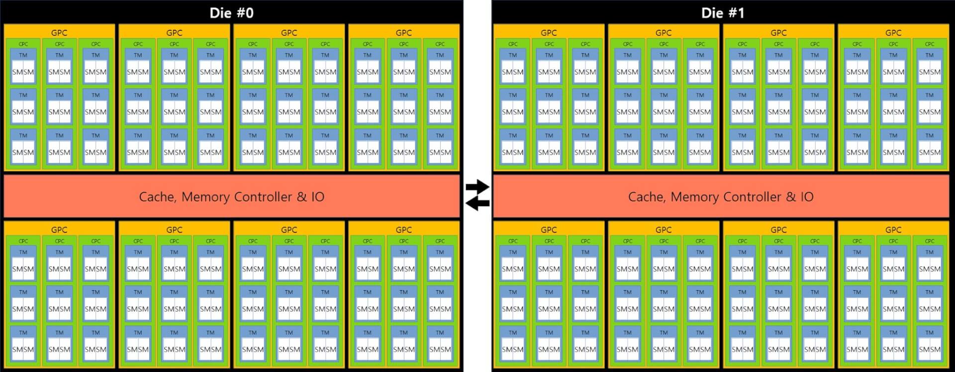
NVIDIA’s also increasing its die size rather significantly. There’s also some info on NVIDIA’s Hopper Data Center graphics cards which are also said to be based on an MCM design. According to @kopit7kimi, every GPC (Graphics Processing Cluster) in the GH100 will consist of three CPCs which in turn will feature three TPCs (Texture Processing Cluster), further sub-divided into two SMs. It’s worth noting that we are expecting a separate architecture for the gaming and data center markets, with Ada Lovelace coming to the former as a monolithic design and Hopper with its MCM design headed to the next-gen Tensor core accelerators. (plpcsanjose.com) Both Hopper and Ada are going to leverage TSMC’s 5nm node, so we expect a notable increase in boost clocks as well.