AMD’s Radeon RX 7900 XT may draw up to 500W of power, rivaling NVIDIA’s next-gen GeForce RTX 4090 not only in terms of performance but power as well. This was revealed by well-reputed leaker @Greymon55 who has proved to be a reliable source in the past. He wasn’t clear regarding this prediction but considering the huge increase in compute density and cache, such a figure isn’t completely surprising even for TSMC’s N5 process.
The Navi 31 (RX 7900 XT) flagship will be based on an MCM (chiplet) design with a total of over 15 thousand cores (15,360 to be exact). It should easily be 2.2-2.5x faster than its predecessor, with the RX 7800 XT (Navi 33) beating the RX 6800 XT by 30-40%.

AMD’s RDNA 3 graphics architecture is expected to get a major overhaul at the front-end, with redesigned Work Group Processors in place of Compute Units, or Dual Compute Units. With RDNA 1 and 2, the WGPs were the basic units for workload scheduling (from CUs on GCN/Vega), but it looks like that is going to change again with Navi 3x. Dual Compute Units are being discarded in favor of wider Work Group Processors, packing as many as 256 stream processors across eight 32-wide SIMDs.
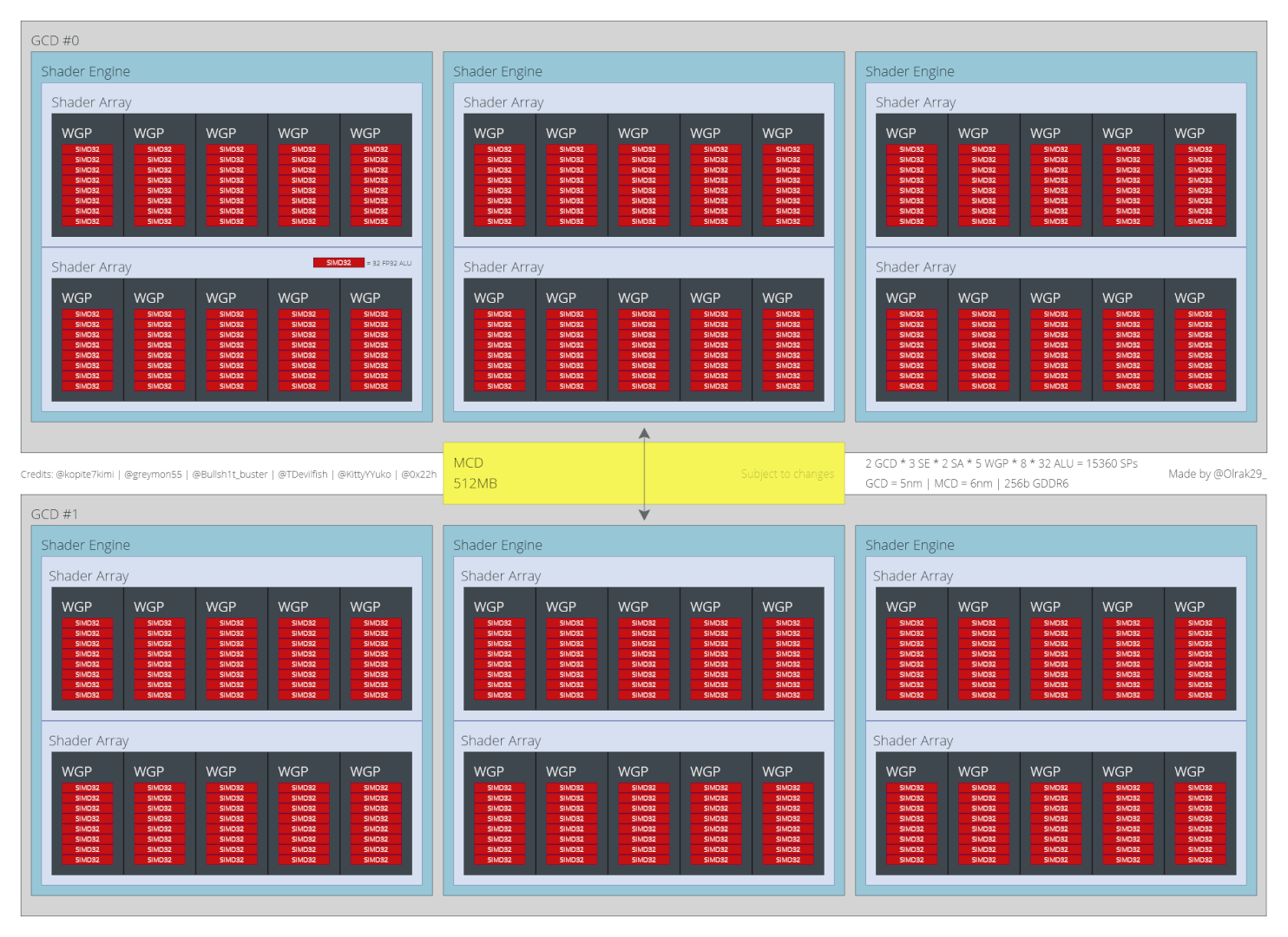
Each Graphics Die (GCD) features three Shader Engines which are made up of two Shader Arrays each. In turn, each Shader Array packs five WGPs containing eight SIMD units (vs four on RDNA 2). The two dies are connected by a bridge interconnect paired with 512MB of L3 “Infinity” Cache. According to the source, the GCDs will be fabbed on TSMC’s 5nm (N5) node while the MCD will be fabbed on the older 6nm (N6) node. Each die should come with a 128-bit bus (divided into eight controllers), resulting in an overall bus width of 256-bit and the same external bandwidth of 448GB/s as the RX 6800 XT/6900XT.
In comparison, Navi 21 featured a Shader Engine packing 10 Dual Compute Units (20 Compute Units) which was in turn divided into two SIMDs per CU or four per DCU. Each CU featured its own vector and scalar units, along with a ray-accelerator, texture mapping units, registers, and cache. Scheduling was done on a WGP (DCU) basis, meaning four wave32 workgroups were assigned at a time. With Navi 3x, scheduling will become more complex as you’re taking 8 SIMDs or wave32 workgroups into account at once.
Navi 32 is also going to be a chiplet design with two compute dies and one MCD. It’ll be a cut-down version of Navi 31, and power the Radeon RX 7800 XT. We’re looking at a core count of around 10,240 shaders (or 40WGP), and a bus width of 192-bit paired with 16GB of GDDR6 memory. The L3 “Infinity Cache” is most likely going to be under 400MB, 384MB is the most probable figure.
According to the latest rumors, the Navi 33 die will pack 4096 shaders (stream processors). It’s expected to power the Radeon RX 7600 XT, making it a massive upgrade over the existing Radeon RX 6600 XT and its 2,304 shaders. We’re looking at an increase of more than 2x if you include the IPC, compute, and frequency gains. The Radeon RX 7600 XT is expected to pack 128-256 MB of Infinity Cache. Rumors indicate a monolithic design, with four 32-bit memory controllers for an overall bus width of 128-bit.
As per rumors, the RTX 4080 and 4090 should offer twice as much performance as the contemporary Ampere parts. The AD102 flagship is rumored to feature 144 SMs distributed across 12 GPCs. That means 18,432 FP32 cores and a peak compute rating of more than 66 TFLOPs, resulting in a 71% gain in raw compute performance over the GA102. Add to that the fact that Team Green is leveraging TSMC’s advanced N5 process node for Lovelace, and the resulting frequency boost should net a ~2.2x gain over the RTX 3090
If the AD102 includes a total of 18,432 cores, we can expect roughly 16,000 cores on the RTX 4080 and 18,000 on the RTX 4090. Considering that we’re likely to see the AD102 fabbed on Samsung’s 5nm/6nm node, the increase in transistor density should absorb the otherwise expected increase in die size.