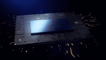
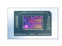
With the launch of the MI200 accelerator, AMD leapfrogged past NVIDIA’s Tesla and Tensor core offerings in one fell swoop. Packing a chiplet based design, incorporating up to 14,080 stream processors across 220 CUs and two dies/chiplets, it is the most advanced accelerator ever designed. Each chiplet features eight shader engineers (total 16) with 16CUs (capable of full-rate FP64 and packed FP32 compute) each and a 2nd Gen Matrix Engine for mixed-precision compute (FP16 and BF16).
Just a few months after the launch of the MI200 and the MI250X, AMD is adding support for the next-gen MI300 range to its ROCm platform. The device IDs of the four chiplets powering the accelerator have been spotted. These are the 0x7408, 0x740C, 0x740F, and 0x7410. This basically confirms earlier rumors stating that the MI300 would feature up to four chiplets, significantly pushing the compute envelope. The MI200 is already a whopping 5x faster than AMD’s A100 Ampere accelerator in FP64 workloads. Doubling the compute capabilities could make it over 10x faster.

Four chiplets mean an overall core count of 28,000, with each die packing 110 Compute Units which in turn, combines 64 ALUs each. 440 CUs across four dies may be a bit too much as one of the key objectives of an MCM approach is to improve yields and bring down production costs. However, even with 80 CU dies, we get a total of 320 CUs across four dies which totals up to a motherlode of 20,480 cores.
In comparison, NVIDIA’s next-gen GH100 “Hopper” accelerator will be limited to 144 SMs or 18,432 FP32 cores, and half as many FP64 cores. It’s expected that Hopper will consist of two GH100 dies paired with over 128GB of 1600MHz HBM3 memory across six 1,024-bit stacks.
| Data Center GPU | NVIDIA Tesla P100 | NVIDIA Tesla V100 | NVIDIA A100 | NVIDIA H100 |
|---|---|---|---|---|
| GPU Codename | GP100 | GV100 | GA100 | GH100 |
| GPU Architecture | NVIDIA Pascal | NVIDIA Volta | NVIDIA Ampere | NVIDIA Hopper |
| SMs | 56 | 80 | 108 | 144x 2 |
| TPCs | 28 | 40 | 54 | 72x 2 |
| FP32 Cores / SM | 64 | 64 | 64 | 64x |
| FP32 Cores / GPU | 3584 | 5120 | 6912 | 9216x 2 |
| FP64 Cores / SM | 32 | 32 | 32 | 32 |
| FP64 Cores / GPU | 1792 | 2560 | 3456 | 4608x 2 |
| INT32 Cores / SM | NA | 64 | 64 | 64 |
| INT32 Cores / GPU | NA | 5120 | 6912 | 9216x 2 |
| Tensor Cores / SM | NA | 8 | 42 | ? |
| Tensor Cores / GPU | NA | 640 | 432 | ? |
| Texture Units | 224 | 320 | 432 | 576x 2 |
| Memory Interface | 4096-bit HBM2 | 4096-bit HBM2 | 5120-bit HBM2 | 6144-bit HBM3? |
| Memory Size | 16 GB | 32 GB / 16 GB | 40 GB | 128GB? |
| Memory Data Rate | 703 MHz DDR | 877.5 MHz DDR | 1215 MHz DDR | 1600 MHz DDR? |
| Memory Bandwidth | 720 GB/sec | 900 GB/sec | 1555 GB/sec | ? |
| L2 Cache Size | 4096 KB | 6144 KB | 40960 KB | 96000 KB? |
| TDP | 300 Watts | 300 Watts | 400 Watts | 500W? |
| TSMC Manufacturing Process | 16 nm FinFET+ | 12 nm FFN | 7 nm N7 | 5 nm N5 |
The GPU in the Linux patch is called Aldebaran with the device ID GF940. Although similar to the GFX90a of the MI250 series, it’s probably a member of the MI300 lineup.
Via: Coelacanth’s Dream