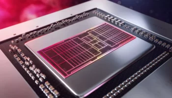
Chinese chipmaker Biren Technology is planning to tape out (finalize design) its first 7nm GPU in the third quarter of this year, with an official launch anticipated in 2022. According to the company’s CTO Mike Hong, the GPU will be designed for training neural networks and machine learning and will go neck to neck against NVIDIA’s next-gen Tensor core GPU (based on the Ada Lovelace microarchitecture). While this is likely going to be a best-case scenario, it’s still a lofty claim, something that won’t materialize in most real-world benchmarks.
This is even more obvious when you consider that the Ampere-based A100 Tensor Core GPU can increase its overall throughput by 20x when using sparsity (a low precision compute format with sparse matrices). Similar to the Tesla GPUs from NVIDIA and the newer A100, Biren’s GPU is aimed at data centers that require support for low-precision compute such as FP16, INT16, and INT8. As such, it won’t be capable of graphics rendering like mainstream GPUs and the graphics pipeline will be replaced by a compute-oriented structure.

The company is looking to leverage data stream processing units and an advanced cache hierarchy with 3D memory packaging (on-die HBM memory) instead of just vector processors that are the basis of traditional GPUs. The former seems to resemble NVIDIA’s DPUs which are a relatively new addition to the data center space and should allow the GPU to be more flexible in terms of its data processing capabilities.
A data processing unit (DPU) is a programmable specialized electronic circuit with hardware acceleration of data processing for data-centric computing. The data is transmitted to and from the component as multiplexed packets of information. A DPU generally contains a CPU, NIC, and programmable data acceleration engines. This allows DPUs to have the generality and the programmability of central processing units while being specialized to operate efficiently on networking packets, storage requests, or analytics requests.
The data acceleration engine differentiates itself from a CPU by a larger degree of parallelism (required to process many requests) and from a GPU by a MIMD architecture rather an SIMD architecture (required as each request needs to make different decisions and follow a different path through the chip). DPUs can be either ASIC-based, FPGA-based, or SoC-based. DPUs have been increasingly used in data centers and supercomputers since their introduction in the 2010s due to the raise to data-centric computing, big data, and artificial intelligence/machine learning/deep learning. DPUs are designed to be independent infrastructure endpoints.[
Wikipedia
Via: CNTechPost